Beware that this post is related to an SDK in maintenance mode
More Info: Consider nRF Connect SDK for new designs

How to generate multiple signals with timing controls (nRF52840)

Hi Nordic community

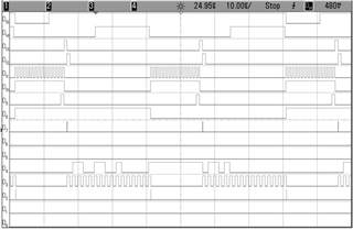
We have a custom IC to interface with the nRF52840 chip. We did testing for that IC with FPGA and the related control, clock signals are as shown in the figure below. The frequency of these signals when interfacing with nRF52840 will be slower, with the highest frequency of 1 MHz. 

It's not too hard to generate these signals with precise timing controls in FPGA but I'm wondering if this is doable with nRF52840? And would you recommend a good strategy to do it (nRF5 SDK or nRF Connect SDK are both fine for us)?

Thanks,

Richard

Parents
  • Hi,

    I can see 15 signal lines here, is this some kind of parallell interface where all signal lines must be in synchronization/timing as shown relative to eachother? Are these bidirection lines or output only? Do I understand it correctly that you must update these pins at up to 1MHz? What can you tell me about other activities the nRF52840 must do (e.g. does it also need to execute Bluetooth or other timing sensitive handling)? 

    Best regards,
    Kenneth

  • Hi Kenneth,

    Thanks for the response. 

    Yes you can say this is parallel interface. Not all signals must be in synchronization but some of them are, meaning some of the edges need to align.

    One pin will be input, others are all output.

    Only a few pins need to update at 1 MHz, but depending on how we update all the signals, 1 MHz is the maximum frequency we need in general.

    We are using quite some resources on the nRF52840. We have other pins used as BLE ANT, I2C, SPI. But I tried to design in such a way that all used pins are kept the maximum possible separation with the ANT pin.

    Please let me know if you need anything else. Hope to hear from you soon.

    Thanks,

    Richard

  • Hi Richard,

    Honestly I think this will be very difficult, from the interrupt latency table you can see that it's not possible to make this interrupt driven, so you will need to make this code run in a tight loop without any other interrupt or even softdevice that can interrupt the execution. If all pins are on the same PORT, you can control them all in one cycle by using the OUT register, if you can allow a 16MHz clock cycles between the signals then you can use the OUTSET and OUTCLR registers after eachother instead (advantage: you don't set/clear pins that is not part of the parallell interface by using those two registers instead of OUT). But honestly speaking I think it's going to be very tight, especially if you need to calculate the parallell output values during the tight timing.

    Best regards,
    Kenneth

Reply
  • Hi Richard,

    Honestly I think this will be very difficult, from the interrupt latency table you can see that it's not possible to make this interrupt driven, so you will need to make this code run in a tight loop without any other interrupt or even softdevice that can interrupt the execution. If all pins are on the same PORT, you can control them all in one cycle by using the OUT register, if you can allow a 16MHz clock cycles between the signals then you can use the OUTSET and OUTCLR registers after eachother instead (advantage: you don't set/clear pins that is not part of the parallell interface by using those two registers instead of OUT). But honestly speaking I think it's going to be very tight, especially if you need to calculate the parallell output values during the tight timing.

    Best regards,
    Kenneth

Children
No Data
Related