
I am working on a power-sensitive project and am interested in minimizing system quiescent currents as much as possible. The project is intended to run off of a coin cell battery for 12-18 months.
We have a SPDT slide button switch that shorts a GPIO input pin to GND or to a second GPIO pin. The second GPIO pin is set in output high mode.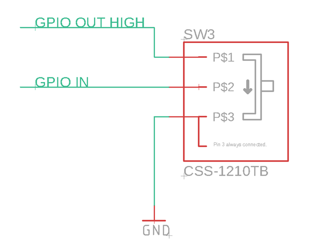
Alternatively, we could replace the output high GPIO pin with a direct connection to V+: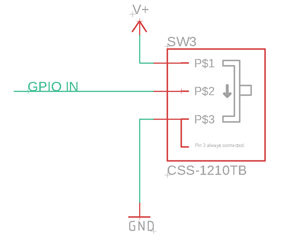
My understanding is that setting the GPIO Output pin HIGH connects the GPIO to V+ through a transistor within the 52810. But, I suspect that there are some parasitic/quiescent effects associated with keeping that pin in output mode to V+.
How much more power is wasted by using a GPIO OUT to the switch, compared to directly connecting it to VDD?
