SHARP Memory Display Breakout - 2.7" 400x240 with nrf52840

Hi,

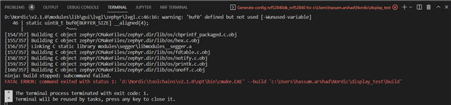
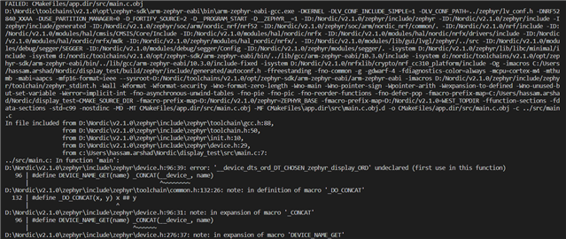
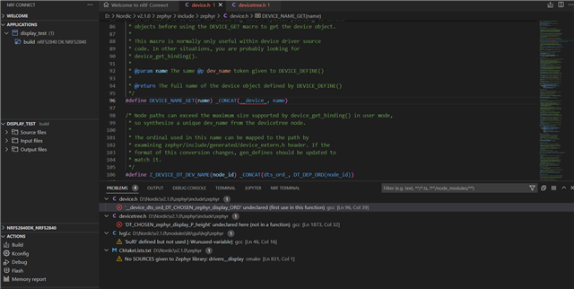
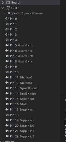
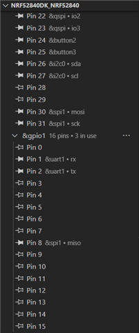
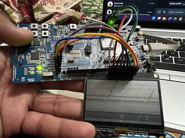
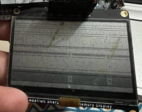
I want to use SHARP Memory Display Breakout - 2.7" 400x240 with nrf52840 development kit. I have to interface the lvgl library for the graphics development but from the documentation, I could not figure out how to connect and there is no basic code for interfacing with the nordic SDK. Please suggest any type of reference for examples if available.

Any kind of input or help will be appreciated.

Thanks in Advance,

Parents
  • Muhammad said:
    Can you guide how I can find which pins are configured for the spi in a specific project?

    After building your project, in the nRF Connect tab, you may expand GPIO to the left in VS Code. However, using the code I uploaded, I was not able to see all pins shown in use as expected. I am assuming this has to do with some of the pins configured using the new Pin control functionality and some pins defined the classic way. I will look into this and get back to you.

  • Hi,

    Thanks for the reply. I have tried with the latest nrfConnect SDK and the following is the error when I open the sample application from the nrfConnect SDK and not a single change. It seems the sample is not compiling fine here.

  • Hi Muhammad,

    At least your output shows that you are now compiling with nRF Connect SDK v2.1.0.

    In the .overlay I provided I accidentally entered default two times(or was it sleep two times). This should be corrected so that the pins are defined for both sleep and default:

    	spi3_default: spi3_default {
    		group1 {
    			psels = <NRF_PSEL(SPIM_SCK, 1, 15)>,
    				<NRF_PSEL(SPIM_MISO, 1, 14)>,
    				<NRF_PSEL(SPIM_MOSI, 1, 13)>;
    		};
    	};
    
    	spi3_sleep: spi3_sleep {
    		group1 {
    			psels = <NRF_PSEL(SPIM_SCK, 1, 15)>,
    				<NRF_PSEL(SPIM_MISO, 1, 14)>,
    				<NRF_PSEL(SPIM_MOSI, 1, 13)>;
    			low-power-enable;
    		};
    	};

    Hopefully, you should now be able to compile the project.

    I have not confirmed whether the overlay will work. It probably only configures the part covered by Pin Control correctly. Some work is needed in order to get the rest of the pins work correctly. I will get back to you over the weekend.

  • Hi,

    Thanks for the information. I have compiled the sample you provided successfully and I have found some results which I want to share as these are not satisfactory at this moment but I think we are now close.

    The pin mapping on the DK was showing following data on the IDE

    Then I have made changes in the spi pin number based on the above the spi3 has 0.14 and 0.15 pins for miso and sck.
    The edited code shown below.

    	spi3_default: &spi3_default {
    		group1 {
    			psels = <NRF_PSEL(SPIM_SCK, 0, 15)>,
    				<NRF_PSEL(SPIM_MISO, 0, 14)>,
    				<NRF_PSEL(SPIM_MOSI, 0, 13)>;
    		};
    	};
    
    	spi3_sleep: &spi3_sleep {
    		group1 {
    			psels = <NRF_PSEL(SPIM_SCK, 0, 15)>,
    				<NRF_PSEL(SPIM_MISO, 0, 14)>,
    				<NRF_PSEL(SPIM_MOSI, 0, 13)>;
    			low-power-enable;
    		};
    	};

    After that, I found the following results on the screen.

    As you can see some number is also shown on the screen and that was updated with time.

    Also, I have connected the rest of the pins as you suggested above. Are there any changes in the pin number which we should make to get a good response?

    What are your suggestions at this stage?

    Do we need to make any changes at this section of the code for the pins to be changed as maybe from the pin mapping picture above you can see pins that are under use and which are free.

        arduino_spi: &spi3 {
            compatible = "nordic,nrf-spim";
            status = "okay";
            cs-gpios = <&arduino_header 16 GPIO_ACTIVE_HIGH>; /* D10 */
            //pinctrl-0 = < &spi3_default >;
            //pinctrl-1 = < &spi3_sleep >;
            //pinctrl-names = "default", "sleep";
        
            ls0xx: ls0xx@0 {
                compatible = "sharp,ls0xx";
                label = "LS0XX";
                spi-max-frequency = <2000000>;
                reg = <0>;
                width = <400>;
                height = <240>;
                extcomin-gpios = <&arduino_header 14 GPIO_ACTIVE_HIGH>; /* D8 */
                extcomin-frequency = <60>; /* required if extcomin-gpios is defined */
                disp-en-gpios = <&arduino_header 12 GPIO_ACTIVE_HIGH>; /* D6 */
            };
        };

    Thanks for all the support.

  • Thank you for the update and photos. It looks like you are getting closer.

    Could you please upload the project files that caused the output seen in the images?

  • Hi,

    Yes, it is your sample as you shared above, I think there were minute changes, I am sharing the version which caused the above output.

    Thanks,

    lvgl_sharp_20221011.zip

  • Thank you for uploading.

    I spotted some other mistakes in the initial suggested pins. (I apologize for the mistake. Please note that the initial suggestions were only meant as a mock up example, demonstrating syntax and how to select pins and making use of Pin control.)

    For example, the following code from the overlay translates to P1.12(not P0.16 as I wrote by mistake):
    cs-gpios = <&arduino_header 16 GPIO_ACTIVE_HIGH>;

    Here is the corrected table:

    Display module pin name nRF52840 pin name Arduino header Comment
    EXTIN P1.04 D3 (Old pin: P0.14)
    DISP P1.05 D4 (Old pin: P0.12)
    EXTMD 'GND' or 'VDD' I assume this is for toggling display inversion.

    CS

    P1.12 D10 (Old pin: P0.16)

    MOSI

    P1.13 D11 Recommend to use P1.13 or another pin as P0.13 may interfere with the LEDs.
    SCLK P1.15 D13 Recommend to use P1.15 or another pin as P0.15 may interfere with the LEDs.
    GND 'GND'
    3V3 'Vin 3-5V' The DK adjusts the IO voltage according to the voltage provided at the 'Vin 3-5V' pin
    VIN (3.3V-5V) '5V' The DK now supplies the display module with 5V
    P1.14 (MISO) D12 MISO not used by display module. Recommended to use P1.14 or another pin as P1.14 may interfere with the LEDs.

    The pins are updated according to the Arduino header definitions in the board files( nrf52840_nrf52840.dts):

    	arduino_header: connector {
    		compatible = "arduino-header-r3";
    		#gpio-cells = <2>;
    		gpio-map-mask = <0xffffffff 0xffffffc0>;
    		gpio-map-pass-thru = <0 0x3f>;
    		gpio-map = <0 0 &gpio0 3 0>,	/* A0 */
    			   <1 0 &gpio0 4 0>,	/* A1 */
    			   <2 0 &gpio0 28 0>,	/* A2 */
    			   <3 0 &gpio0 29 0>,	/* A3 */
    			   <4 0 &gpio0 30 0>,	/* A4 */
    			   <5 0 &gpio0 31 0>,	/* A5 */
    			   <6 0 &gpio1 1 0>,	/* D0 */
    			   <7 0 &gpio1 2 0>,	/* D1 */
    			   <8 0 &gpio1 3 0>,	/* D2 */
    			   <9 0 &gpio1 4 0>,	/* D3 */
    			   <10 0 &gpio1 5 0>,	/* D4 */
    			   <11 0 &gpio1 6 0>,	/* D5 */
    			   <12 0 &gpio1 7 0>,	/* D6 */
    			   <13 0 &gpio1 8 0>,	/* D7 */
    			   <14 0 &gpio1 10 0>,	/* D8 */
    			   <15 0 &gpio1 11 0>,	/* D9 */
    			   <16 0 &gpio1 12 0>,	/* D10 */
    			   <17 0 &gpio1 13 0>,	/* D11 */
    			   <18 0 &gpio1 14 0>,	/* D12 */
    			   <19 0 &gpio1 15 0>,	/* D13 */
    			   <20 0 &gpio0 26 0>,	/* D14 */
    			   <21 0 &gpio0 27 0>;	/* D15 */
    	};

Reply
  • Thank you for uploading.

    I spotted some other mistakes in the initial suggested pins. (I apologize for the mistake. Please note that the initial suggestions were only meant as a mock up example, demonstrating syntax and how to select pins and making use of Pin control.)

    For example, the following code from the overlay translates to P1.12(not P0.16 as I wrote by mistake):
    cs-gpios = <&arduino_header 16 GPIO_ACTIVE_HIGH>;

    Here is the corrected table:

    Display module pin name nRF52840 pin name Arduino header Comment
    EXTIN P1.04 D3 (Old pin: P0.14)
    DISP P1.05 D4 (Old pin: P0.12)
    EXTMD 'GND' or 'VDD' I assume this is for toggling display inversion.

    CS

    P1.12 D10 (Old pin: P0.16)

    MOSI

    P1.13 D11 Recommend to use P1.13 or another pin as P0.13 may interfere with the LEDs.
    SCLK P1.15 D13 Recommend to use P1.15 or another pin as P0.15 may interfere with the LEDs.
    GND 'GND'
    3V3 'Vin 3-5V' The DK adjusts the IO voltage according to the voltage provided at the 'Vin 3-5V' pin
    VIN (3.3V-5V) '5V' The DK now supplies the display module with 5V
    P1.14 (MISO) D12 MISO not used by display module. Recommended to use P1.14 or another pin as P1.14 may interfere with the LEDs.

    The pins are updated according to the Arduino header definitions in the board files( nrf52840_nrf52840.dts):

    	arduino_header: connector {
    		compatible = "arduino-header-r3";
    		#gpio-cells = <2>;
    		gpio-map-mask = <0xffffffff 0xffffffc0>;
    		gpio-map-pass-thru = <0 0x3f>;
    		gpio-map = <0 0 &gpio0 3 0>,	/* A0 */
    			   <1 0 &gpio0 4 0>,	/* A1 */
    			   <2 0 &gpio0 28 0>,	/* A2 */
    			   <3 0 &gpio0 29 0>,	/* A3 */
    			   <4 0 &gpio0 30 0>,	/* A4 */
    			   <5 0 &gpio0 31 0>,	/* A5 */
    			   <6 0 &gpio1 1 0>,	/* D0 */
    			   <7 0 &gpio1 2 0>,	/* D1 */
    			   <8 0 &gpio1 3 0>,	/* D2 */
    			   <9 0 &gpio1 4 0>,	/* D3 */
    			   <10 0 &gpio1 5 0>,	/* D4 */
    			   <11 0 &gpio1 6 0>,	/* D5 */
    			   <12 0 &gpio1 7 0>,	/* D6 */
    			   <13 0 &gpio1 8 0>,	/* D7 */
    			   <14 0 &gpio1 10 0>,	/* D8 */
    			   <15 0 &gpio1 11 0>,	/* D9 */
    			   <16 0 &gpio1 12 0>,	/* D10 */
    			   <17 0 &gpio1 13 0>,	/* D11 */
    			   <18 0 &gpio1 14 0>,	/* D12 */
    			   <19 0 &gpio1 15 0>,	/* D13 */
    			   <20 0 &gpio0 26 0>,	/* D14 */
    			   <21 0 &gpio0 27 0>;	/* D15 */
    	};

Children
  • Hi,

    Thanks for the reply. I have tried as you said above and tried after verification as well multiple times. But the results are the same as there is no display on the screen. Do you know what could be the reason?


    Also, currently, I am connecting Vin of lcd with DK 5v pin and v3.3 with VDD of DK. Do you think we need to provide the lcd a separate voltage source? if yes on which pin?

  • What is the voltage operating range specification of the display? What is the recommended operating voltage, and what is the IO voltage levels of the display?

    Muhammad said:
    Also, currently, I am connecting Vin of lcd with DK 5v pin and v3.3 with VDD of DK.

    If the LCD is powered with 5V, you might need to power the DK with a higher voltage as well, in order for the IO signals to match.

    The nRF52840 DK can be configured for 5V mode using the nRF power source switch on the DK. Set the switch to 'USB'.

    More details about this switch in the DK user guide.

    Muhammad said:
    But the results are the same as there is no display on the screen. Do you know what could be the reason?

    Are you still seeing '52', like the image below, or is the screen completely blank? Is the screen dark or bright? Does it change when you power it?

    Do you have access to any logic analyzer or oscilloscope? If so, you could check whether there is activity on the pins as expected.

  • Hi,

    After you have send me the updated pin configurations I can not now see the 52 on screen instead there are black lines on screen. I also have tried to give the 5V power to the screen but there were no results.

  • Is there any output to the terminal? The terminal could be outputting logs and error codes from the application.

    Did you check the pins to see whether there is any activity?

  • Hi,

    No there was no activity on the terminal and also I tried to debug. During the debugging the application seems to be running smooth and there were no exceptions or breakage.

    Also on the pins there was some activity and seems that data is going through it but not sure if its right or not.

    Is there any pin that we are missing to enable or attach?

Related