
Hi,
I'm designing a drone based on these three Nordic IC:
- nPM1100
- nRF5340
- nRF21540
Let's Start with nPM1100:
Based on this Reference circuitry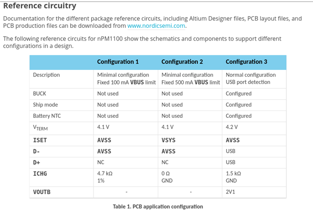
I based my design on Configuration 3: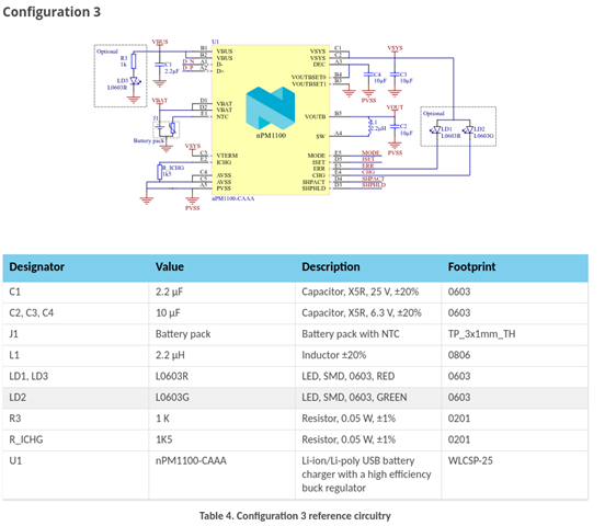
This is my schematic on KiCAD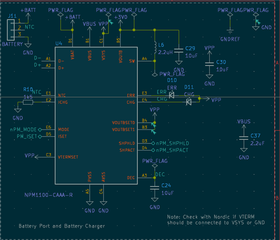
I connected VTERM to VPP
However, checking the schematics on the Thingy53 I see the VTERM Connected to GND: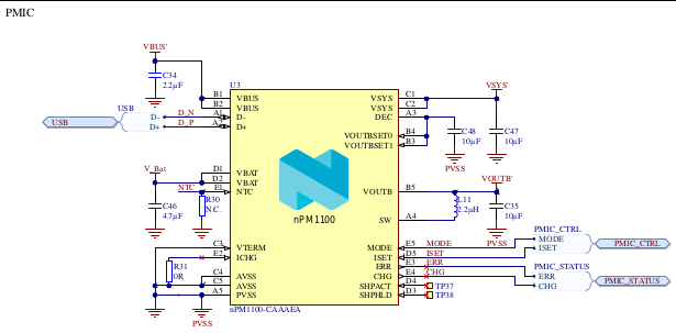
Is there any particular reason the VTERM is connected on GND instead of VPP?
Furthermore, I see both VOUTBSET0 and VOUTBSET1 connected to DEC. This should be any problem cause internally DEC is connected to VSYS: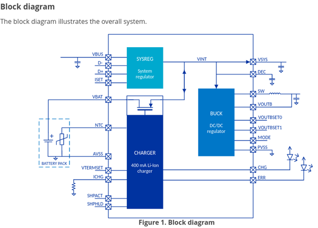
For this PCB connection I wonder is the GND plane around the nPM1100 is ok or needs to be clear out a little bit?
Suggestions? 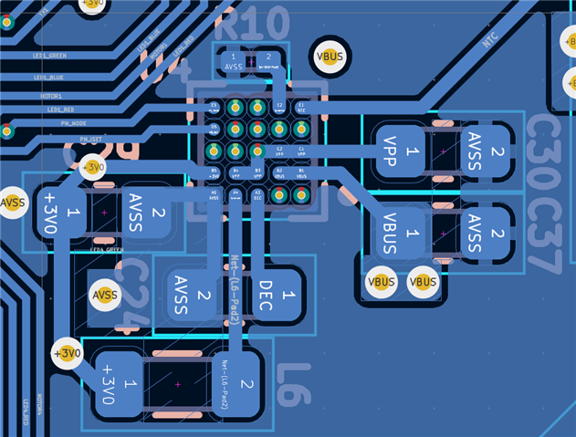
About the nRF5340 the questions I got are related to the RF signal connected to nRF21540.
nRF5340 schematic: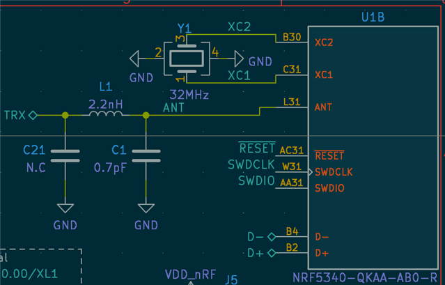
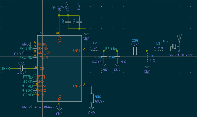
nRF21540 schematic:
PCB: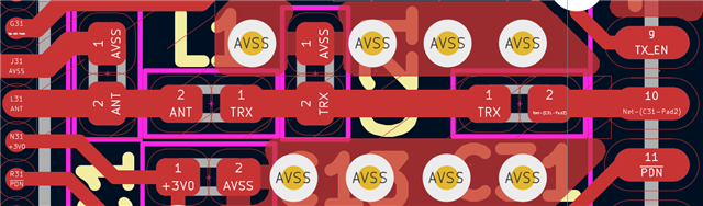
These components are placed quite close together.
I'm been tinkering around the RF signal width base on different stack up
My current stack up is this: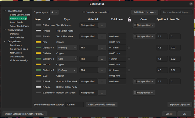
KiCAD calculator indicates this for Microstrip Line: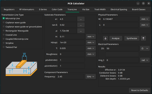
And this for Coplanar Wave Guide:
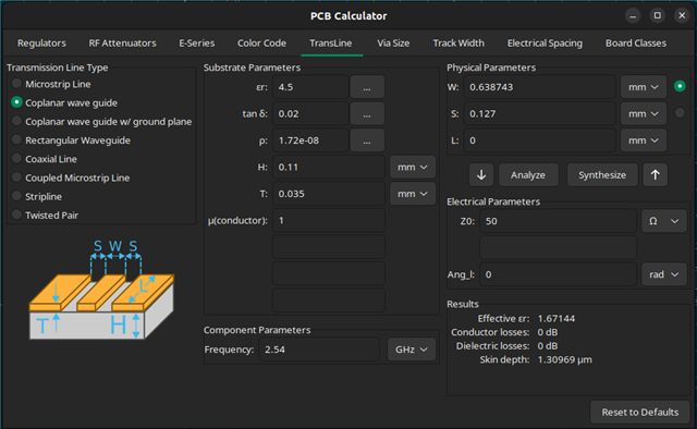
And this for Coplanar Wave Guide with ground plane:
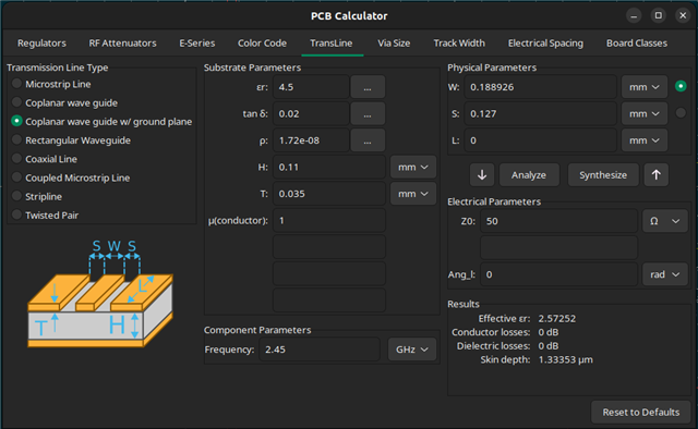
I think I should use the last one because I got a 4 Layer PCB with GND plane just below RF signal plane, however I'm not sure about the trace width.
Suggestions?
About nRF21540 both schematics and PCB for single antenna.
Checking the documentation on https://infocenter.nordicsemi.com/index.jsp?topic=%2Fstruct_protplatforms%2Fstruct%2Fprotplatforms.html&cp=14
I see two things I want to validate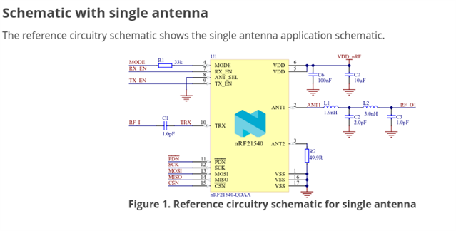
First the resistor R1/33k connected in serie with MODE pin.
Checking this documentation Errata: https://infocenter.nordicsemi.com/index.jsp?topic=%2Fps_nrf21540%2Fchapters%2Fproduct_overview%2Fdoc%2Ffrontpage.html&cp=7_0_0_2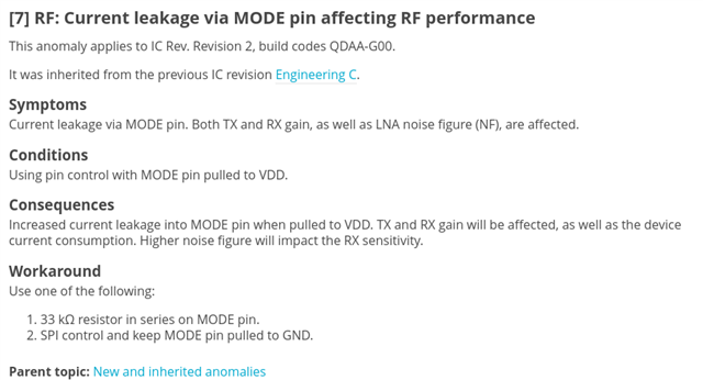
I decided to go for option Number 2 and connect the MODE pin to GND.
The second thing that got my attention is the 50R resistor connected to the ANT2.
Based on Thingy53 schematics: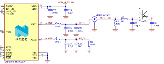
I wonder if the LC network connected between the 49R9 and the ANT2 is mandatory or it's something I don't really needs for my design.
About the Chip Antenna, the Thingy52 use a different SMD Chip Antenna
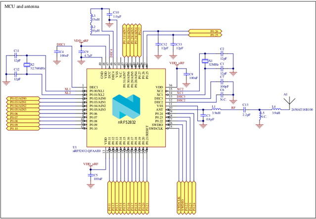
I wonder if the Chip Antenna 2450AT18B100 can be used with the nRF21540 or should I change the Chip Antenna for WLA.01 used on the Thing53?:
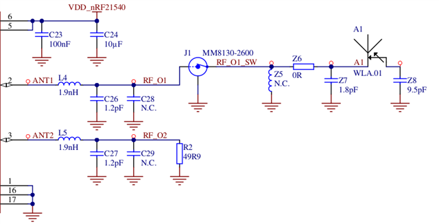
Furthermore, Is needed the RLC network connected after the MM8130-2600, even when I don't use that connector on my design?
Lastly, the PCB components placement for LC network connected to ANT1 and ANT2:
The Thingy53 got this PCB design: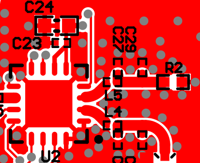
I currently have this one: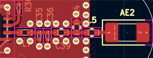
Should I move the LC network move down or should I keep it as it is?
Thanks and Best Regards,
Jose Pablo (JP) Castro Valverde

