
Hi, I am working on a pcb design utilising the nrf52840. I want to use a pcb antenna. I am a hobbyist so It’s very likely I’m misunderstanding something. I am interested in using the ¼ wave monopole like the nrf52840DK antenna design instead of the meander style antenna on the nrf52840 dongle for the normal reasons, easy to tune, the board will have enough space, sounds like it might be more forgiving with manufacturer tolerances etc.
I have read the frequently referenced white paper (l/4 printed monopole antenna for 2.45GHz), it assumes a dielectric constant of 4.4 for 1.6mm FR4 but doesn’t explain what to do if the dielectric constant is different. I want to go through JLCPCB which suggest a dielectric constant of 4.5 for their 2-layer boards. Will this make a big difference? Also, the white paper suggests the antenna has a width of 1.5mm, however, the nrf52840DK antenna is 1.25mm, is the width important?
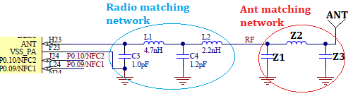
The matching network on the chip side of both the DK and the dongle are the same. However, the matching network at the antenna end of the DK and the dongle are different, 1.2pF & 1.5pf capacitors respectively. Which should I use for a 2-layer board with a printed ¼ wave monopole antenna? is this value based on the antenna type, or build up of the board? or is it a combination of all things and requires tuning to get “perfect”?
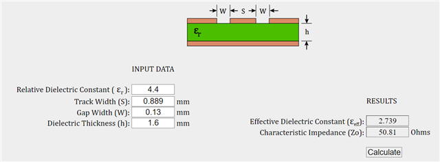
Last question for this post. The dongle has a grounded coplanar wave transmission line dimensions entered below which basically gives the target 50 ohms.
However, the DK grounded coplanar wave transmission line dimensions entered below are way off 50 ohms.
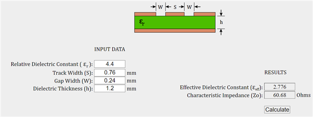
Is there a reason for this or have I got something very wrong/misunderstood?
Any help on the above matters is appreciated, thank you.
J

 - example with nRF52833 and antenna.