nRF52832_PCB_module_v2.zipcustom_symbols_footprints.zip
Hi,
I'd like to have a HW review.
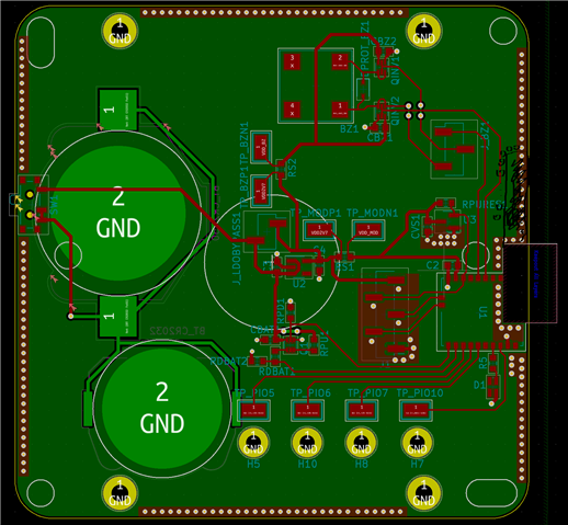
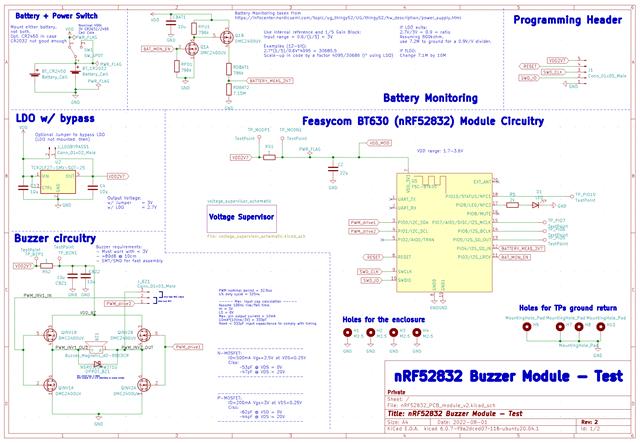
I have designed a PCB around the FSC-BT630 module which includes the nRF52832.
I have included all the files necessary for your to check it out in KiCAD v6.
Goals:
- Have a low-power buzzer module that I can turn on/off from a distance (10-20m).
- A regular smartphone will be the intended client.
- Flexibility for testing different settings:
- CR2032 or CR2450 battery
- Self-driving H-bridge for buzzer or differential driving from 2 module PWM pins.
- Coarse estimation of battery capacity
- Test whether an LDO is needed or not (either use jumper or LDO, but not both)
Details:
- The size of the PCB was designed for a Candemboss CBRS01V enclosure.
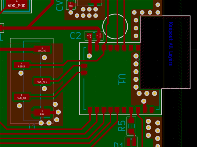
- Programming pin-header w/ VDD2V7, RESET, SWD_CLK, SWD_IO and GND
- Grounded holes for enclosure
- 2-layer board with signal and ground layers.
- FSC-BT630 module
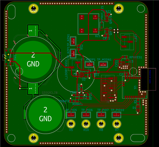
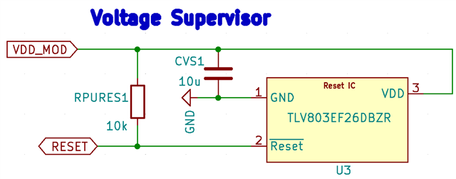
Here are some of the relevant screenshots of my design:
Questions:
- For via shielding around antenna, I assumed 5GHz as the highest frequency (2x2.55GHz). Using the lambda/20 rule-of-thumb, it came out to be 1.4mm. Is this overkill (i.e. should've just used 2.5GHz or is it a safe assumption?
- Is it possible to program this board from a nRF52832 or nRF52840 DK board?
- Should I add more via stitching around the board?
Please, let me know if you need anything else.
Thanks in advance!