Issues with programming/operation of custom PCB with nRF52832

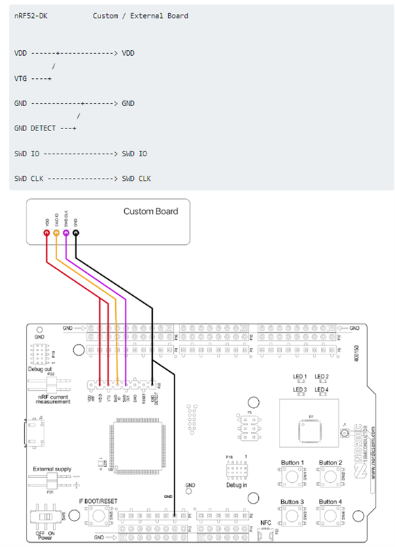
I've just built up a batch of custom PCB's we designed using the nRF52832-QFAA IC's.  I'm attempting to program these with the nRF52-DK, and am following the connection diagram indicated below, with the exception that I have not got the GND_DETECT connected, as I am led to believe this is not necessary.

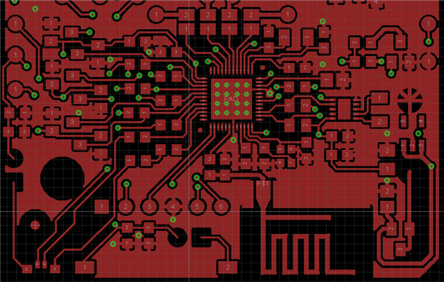
My custom board is designed around the Internal LDO reference design in the nRF52832 Product Specification, and looks like this:

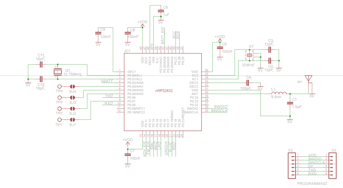
My 32MHz Xtal has 8pF load capacitance, ESR = 80 ohms and shunt capacitance of 3pF, which appears to be within spec according to the spec for the 64 MHz crystal oscillator (HFXO).

I have erased the nRF52 chip on my DK, so that (I assume) it lets all the GPIO float.  And then I have programmed my custom board with a simple LED blinky program.  Testing of this LED Blinky on the nRF53-DK indicates it is working as expected, but when I flash my custom board, I'm not seeing anything on the appropriate GPIO pin.

I've tested both powering my custom board via the DK, and also powering the custom board from an external PSU.  Checking the current indicates a load of 4-7mA, which seems a bit high. 

Poking around on some other GPIO, I noticed that P0.05 is being switched on/off at about 2200Hz, with a pulse width of ~ 7usec.

I programmed and tested a second production board, and that showed the same behaviour.

I then tested a board that was straight off the production floor and hadn't been programmed, and that wasn't doing anything (as I'd expect).

So, for some reason, code is being flashed to the device, but its not the code I am expecting to be flashed to the device.  I'm trying to toggle P0.17 at about 1Hz with a 50% duty cycle, but instead I'm seeing P0.05 toggle at about 2200Hz with a ~ 2% duty cycle!

Does anyone have any idea what I'm doing wrong?

Cheers,

Mike

Parents
  • Did some more work on this today:

    1) Swapped out the 32MHz Xtal on my custom board with the 32MHz xtal off my DK and re-tested.  The DK worked with the 32MHz xtal off my custom board but my custom board isn't working with the 32MHz xtal off the DK

    2) Had a detailed look at the recommended layout as per the DK documentation.  The only thing I've done differently that might be an issue is that I've not made the VSS connection to Pin 31 in the recommended way.  But I can't see that preventing the chip from functioning at all.

    I've got a 4 layer PCB with GND pours on the bottom layer, top layer and layer 2.  I've also got a pour on layer 3 that is connected to VDD.

    Screen shots of the layout around the chip are shown below:

    Top Layer:

    Layer 2 (GND Pour):

    Layer 3 (VDD pour):

    Bottom Layer (GND pour):

    Regards,

    Mike

Reply
  • Did some more work on this today:

    1) Swapped out the 32MHz Xtal on my custom board with the 32MHz xtal off my DK and re-tested.  The DK worked with the 32MHz xtal off my custom board but my custom board isn't working with the 32MHz xtal off the DK

    2) Had a detailed look at the recommended layout as per the DK documentation.  The only thing I've done differently that might be an issue is that I've not made the VSS connection to Pin 31 in the recommended way.  But I can't see that preventing the chip from functioning at all.

    I've got a 4 layer PCB with GND pours on the bottom layer, top layer and layer 2.  I've also got a pour on layer 3 that is connected to VDD.

    Screen shots of the layout around the chip are shown below:

    Top Layer:

    Layer 2 (GND Pour):

    Layer 3 (VDD pour):

    Bottom Layer (GND pour):

    Regards,

    Mike

Children
  • Hello Mike,

    The design looks ok. The decoupling capacitor are a bit from the SoC, this might have some deviation from the design in layout. However it's not critical problem, we guess. 

    You do not have DCDC in the design. But DK has. So you need to disable the DCDC in the application before programming the device. 

    CONFIG_BOARD_ENABLE_DCDC=n


    Thanks.

    Best Regards,

    Kazi Afroza Sultana

  • Hi Kazi,

    I did in fact try that earlier, and it made no difference to the functioning of my custom board.

    I did some more digging with the Ozone debugger.  This is what I have discovered:

    According to this: https://infocenter.nordicsemi.com/index.jsp?topic=%2Fcom.nordic.infocenter.nrf52832.ps.v1.1%2Fgpio.html  the address of the GPIO IN Register that shows the status of all the GPIO pins at any point is 0x50000510.  I am trying to toggle P0.18 on my hardware.  This is what I see at that memory location within the Memory Window of Ozone with the relevant GPIO (P0.18) pulled low (so the LED turns on)

    50000500  00 00 00 00 60 00 00 00 60 00 00 00 60 00 00 00

    50000510 C0 01 20 00 60 00 04 00 60 00 04 00 60 00 04 00 

    And again with relevant GPIO (P0.18) pulled high (so the LED turns off):

    50000500  00 00 00 00 60 00 04 00 60 00 04 00 60 00 04 00

    50000510  C0 01 20 00 60 00 04 00 60 00 04 00 60 00 04 00

    So I can’t quite make sense of the actual bytes that are changing and correlate that to the relevant GPIO.  But at least it looks like the relevant registers are being updated.

    And the bizarre thing is, I am now seeing the correct activity on the relevant GPIO pin!

    However, if I stop debugging, and flash the custom board with the same firmware I was using during debugging, but don’t run the debugger, then I am not seeing any activity on the GPIO.

    Any ideas why this might be occurring?

    Regards,

    Mike

Related