I am using nRFConnect for desktop to program bootloader / softdvice / application.
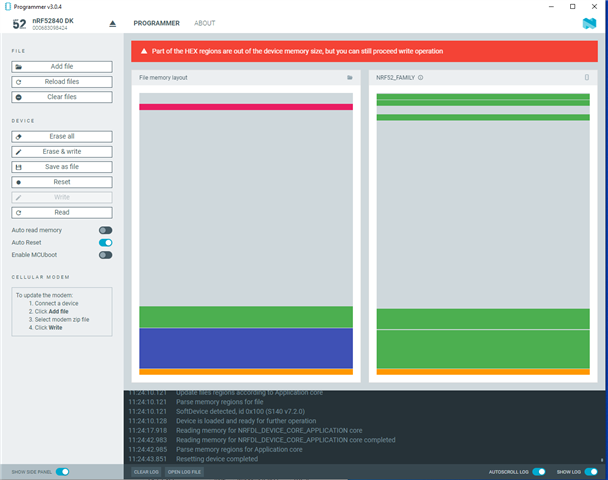
After programming the images I click the read button to see what the layout looks like - see attached image.
The right side of the display shows the NRF52_FAMILY layout.
At the top there are two small green areas.
topmost green area: FF000 - FF37F 896 bytes. Region Name: Application
next lower green area: FE000-FE37F 896 bytes. Region Name: Application
Then
next lower green area: 27000-3ABFF 80896 bytes. Region Name: Application
What are those two 896-byte areas for and why are they both the same size? Should there be two?
Linker info:
linker_section_placement_file="flash_placement.xml"
linker_section_placement_macros=
FLASH_PH_START=0x0
FLASH_PH_SIZE=0x100000
RAM_PH_START=0x20000000
RAM_PH_SIZE=0x40000
FLASH_START=0xf5000
FLASH_SIZE=0x9000
RAM_START=0x20005978
RAM_SIZE=0x3a688
linker_section_placements_segments=
FLASH1 RX 0x0 0x100000
RAM1 RWX 0x20000000 0x40000
mbr_params_page RX 0x000FE000 0x1000
bootloader_settings_page RX 0x000FF000 0x1000
uicr_bootloader_start_address RX 0x10001014 0x4
uicr_mbr_params_page RX 0x10001018 0x4
Overall does this memory layout look correct?