Hello!
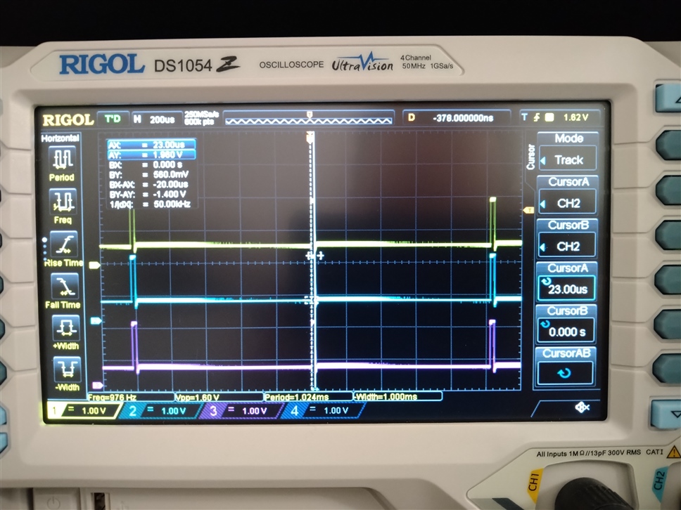
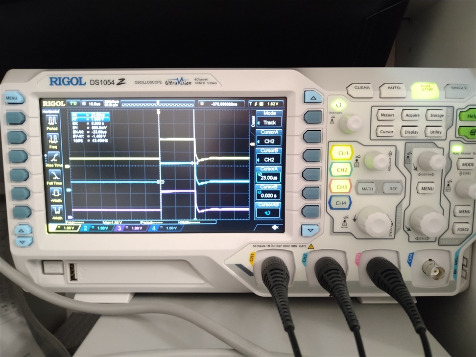
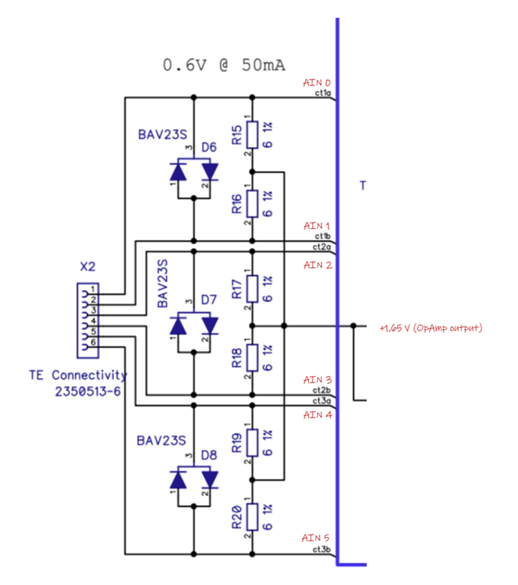
We are using a custom nRF9160 board with 3 differential ADC channels. The differential voltage is measured across two resistors, with the center voltage (normally OpAmp driven) at 1,66 V.
I'm sampling three ADC channels in differential mode and noticed weird results and verified with a scope: Taking a sample with more than one channel enabled results in nRF9160 connecting the ADC-inputs to what appears to be VDD-ish for a period that seems to be TACQ*2. Sampling is triggered by PPI, currently at 1 kHz, and this phenomenon happens at every sample. (Changing the PPI frequency changes the spike positions as well.
Changing to single-ended measurement makes no difference but the problem doesn't show on scope with only one channel enabled.
Do I have something wrong with my SAADC configuration?
UPDATE 2022-10-24: Issue is related to CONFIG_BOOTLOADER_MCUBOOT and pin P0.14, which seems to configured as output and connecting to VDD_GPIO when it is sampling ADC
// SAADC Channel configuration
#define ADC_CONFIG_DIFF (SAADC_CH_CONFIG_GAIN_Gain1     << SAADC_CH_CONFIG_GAIN_Pos) | \
                        (SAADC_CH_CONFIG_MODE_Diff        << SAADC_CH_CONFIG_MODE_Pos) | \
                        (SAADC_CH_CONFIG_REFSEL_Internal  << SAADC_CH_CONFIG_REFSEL_Pos) | \
                        (SAADC_CH_CONFIG_RESN_Bypass      << SAADC_CH_CONFIG_RESN_Pos) | \
                        (SAADC_CH_CONFIG_RESP_Bypass      << SAADC_CH_CONFIG_RESP_Pos) | \
                        (SAADC_CH_CONFIG_TACQ_10us        << SAADC_CH_CONFIG_TACQ_Pos)
static void init_adc(void) {
  NRF_SAADC_NS->TASKS_CALIBRATEOFFSET = 1;

  NRF_SAADC_NS->RESOLUTION = SAADC_RESOLUTION_VAL_12bit;

  // Set sampling rate to be controlled by "SAMPLE", call.
  NRF_SAADC_NS->SAMPLERATE = SAADC_SAMPLERATE_MODE_Task;

  //Set the EasyDMA buffer
  active_buffer = 0;
  NRF_SAADC_NS->RESULT.PTR = (uint32_t) &m_sample_buffer_0;
  NRF_SAADC_NS->RESULT.MAXCNT = ADC_TOTAL_BUFFER_LEN;

  // Enable interrupt for buffer full
  NRF_SAADC_NS->INTENSET = SAADC_INTENSET_END_Set << SAADC_INTENSET_END_Pos;
  NRF_SAADC_NS->INTEN |= SAADC_INTEN_END_Enabled << SAADC_INTEN_END_Pos;
  NRF_SAADC_NS->EVENTS_END = 0;

// Configure SAADC Channels
  NRF_SAADC_NS->CH[0].CONFIG = ADC_CONFIG_DIFF;
  NRF_SAADC_NS->CH[0].PSELP = SAADC_CH_PSELP_PSELP_AnalogInput0 << SAADC_CH_PSELP_PSELP_Pos;
  NRF_SAADC_NS->CH[0].PSELN = SAADC_CH_PSELN_PSELN_AnalogInput1 << SAADC_CH_PSELN_PSELN_Pos;


  NRF_SAADC_NS->CH[1].CONFIG = ADC_CONFIG_DIFF;
  NRF_SAADC_NS->CH[1].PSELP = SAADC_CH_PSELP_PSELP_AnalogInput2 << SAADC_CH_PSELP_PSELP_Pos;
  NRF_SAADC_NS->CH[1].PSELN = SAADC_CH_PSELN_PSELN_AnalogInput3 << SAADC_CH_PSELN_PSELN_Pos;


  NRF_SAADC_NS->CH[2].CONFIG = ADC_CONFIG_DIFF;
  NRF_SAADC_NS->CH[2].PSELP = SAADC_CH_PSELP_PSELP_AnalogInput4 << SAADC_CH_PSELP_PSELP_Pos;
  NRF_SAADC_NS->CH[2].PSELN = SAADC_CH_PSELN_PSELN_AnalogInput5 << SAADC_CH_PSELN_PSELN_Pos;


  NVIC_EnableIRQ( SAADC_IRQn );
  NVIC_SetPriority( SAADC_IRQn, 1UL );
  IRQ_DIRECT_CONNECT(SAADC_IRQn, 0, SAADC_IRQHandler, 0);
  NRF_SAADC_NS->ENABLE = 1;
}
Scope images (OpAmp off, resulting in ~0,7 V average at the OpAmp output)