Write verify fails on custom nRF52810 board

I've put the recommended circuit for the nRF52810 QCAA chip together on breadboard (schematic is below) and am using a J-Link Edu Mini to program.
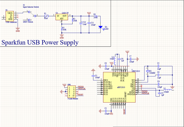
I created a custom board template in nRF Connect with nrf52810 QFAA (no QCAA option) and used it to build both Hello World and Blinky examples. When I try to flash either example I receive a "ERROR: Write verify failed." message which expands to:

[error]: [ nRF52] - Data does not match in address range [0x00000000-0x00007a30] (Flash)

[error]: [ nRF52] - Expected byte value 0xfe but read 0x00 at address 0x000029f0.

[error]: [ nRF52] - Flash verification failed.

[error]: [ nRF52] - Failed while verifying file c:\ncs\Applications\hello_world\build_1\zephyr\zephyr.hex.

with the log command.

I've also used an nRF52 devkit build (with the NRF52810 version selected) and received a similar message with different values:

[error]: [ nRF52] - Data does not match in address range [0x00000000-0x00008b40] (Flash)

[error]: [ nRF52] - Expected byte value 0xf0 but read 0x00 at address 0x000011e1.

[error]: [ nRF52] - Flash verification failed.

[error]: [ nRF52] - Failed while verifying file c:\ncs\Applications\hello_world\build\zephyr\zephyr.hex.

I was able to flash this build to the actual dev board hardware fine.

I've attached the log file from this devkit build.

Any help would be appreciated Slight smile

Thanks

1200.log.log

Parents
  • Hi

    What is the supply voltage of your board? 

    The J-Link Edu Mini does not have level shifters on board, and as such will only be able to program boards with a supply voltage of around 3.3V. 

    If your board is using a different supply voltage you would need to use something like the J-Link Base, which supports the entire voltage range of the nRF52 devices. 

    Best regards
    Torbjørn

  • Hi Torbjorn,

    Thanks for the reply.

    The voltage supply to the board is 3.3V.

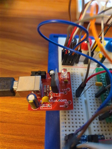
    Here's a picture of the supply itself.

  • Hi,

    I tried adding the command you suggested and got the same result.

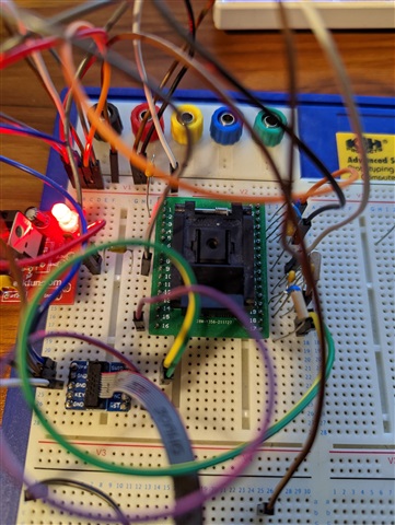
    The board is messy unfortunately but here's an image:

    The VDD pins all show roughly 3.3V, DEC1 shows 1.1V and DEC2 shows 1.3V.

    I've double checked the capacitor on DEC1 and it is definitely 100nF so I'm not sure why it is at 1.1V.

    Thanks

  • Hi 

    Running the chip from a socket like this, with all the external components hooked up on a breadboard, is more or less guaranteed to fail unfortunately. 

    The long connections between the pads on the chip and the components will add a lot of capacitance to the signals, which will affect the operation of the device. 

    Is your end goal to make your own PCB?
    If so I would recommend getting an nRF52DK for development. 

    The nRF52DK uses the nRF52832 rather than the nRF52810, but we don't have a dedicated DK for the nRF52810. When developing your code it is possible to limit the project to the resources of the nRF52810, even if the nRF52832 is used for development. 

    If your end goal is just to run something from a breadboard I would look for an nRF52810 module that has the right pitch and placement of GPIO's so that it can be connected to the breadboard easily. For a full list of 3rd party modules using the nRF52810 please have a look here

    Best regards
    Torbjørn

  • That...makes perfect sense now that you mention it.

    My end goal is to make a PCB but I had the idea to fully prototype it first to aviod any issues with the final design. I can see why that isn't an option now though.

    I have had the nRF52DK for a while now so I will just use that instead.

    I really appreciate youir help Torbjørn, thanks a lot.

  • Hi 

    Breadboarding works for simple circuits using low frequency signals, but high frequency signals like crystal oscillators and RF signals will not. 

    The most important advice I can give on PCB design is to copy our reference design as much as you can, in particular the RF part. For a 2.4GHz signal just one millimeter of extra trace adds 1 nH of inductance, meaning the simple act of moving a component and lengthening the trace will dramatically change the characteristics of your board. 

    The second piece of advice I will provide is to keep in touch with us in support. Once you have your schematic ready please send it to us for review, and the same when you have your layout ready. Then you greatly maximize the chance of having something working when you get your PCB manufactured. 

    More information on PCB design guide lines and reference layout for the nRF52810 can be found here.

    Best regards
    Torbjørn

  • Thank you for the extra info, I haven't done high frequency layout before so this is all good to know.

    I will definitely send in my schematic and layout when I've completed them, I didn't realise it was an option honestly but I'm very happy to know I can get more help if (when Slight smile) something goes wrong.

    Thanks again for all the help.

Reply Children
Related