Hello,
We're currently developing PCB with nRF5340_CLAA SoC. For specific reasons, main supply voltage was changed from stable 3.3V to 3.5V that comes from DC/DC converter.
Voltage in some scenarios can goes up to 3.7-3.8V for few miliseconds when Converter is in startup phase. As previously we consider to set nRF53 in normal voltage mode (DC/DC), now It looks like we have to change operation mode to high-voltage DC/DC mode.
Therefore, I have a few questions that I cannot find or understand in the technical documentation.
- When nRF53 is set to HV mode, VDDH pin is the only one Voltage Input Pin? What is the current efficiency of this input?
- We will not use VBUS pin as device will not have USB functionality and external Power Supply will be managed from external components.
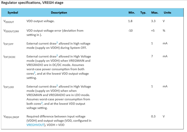
- When nRF53 is set to HV mode, do VDD inputs become voltage outputs or needs to be connected to main supply voltage together with VDDH?
- What is the maximum constant current of internal VREGH regulator available to supply external devices?
Best Regards,
Lukasz