Bluetooth antenna design

This is my first design with a BT product so apologies if my quest is a little simple.


The advice I was initially given was just to cop the dev board design and it “should work”


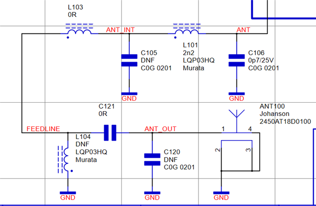
This issue I have is that the space constraints on the PCB are making using that exact bit very difficult and it is a large bit of PCB area.

If this is the case how exact to the design does it need to be?


I know I can design another PCB antenna but then how long would validation of that design take as it is now different from the dev board layout. Also as mentioned this is not only my first design of a BT device but no one else in my company has done his before.


Equally I could you a chip antenna, but I don’t understand the time frames for extra design or validation of any part chosen?


If anyone has any useful guidance on which way to go as I have a very tight deadline to meet to deliver this board


Many thanks

  • Hi,

    The easiest solution is to use a chip antenna. The antenna manufacturers have footprint and clearance area recommendations which should be followed, so including a chip antenna into the design only consist of copying the dimensions listed in the antenna datasheet.

    We are using a chip antenna from Johanson technologies on the nRF21540DK, they have a antenna selection guide that helps with finding the antenna best suited for your application:

    https://www.johansontechnology.com/chip-antenna-selection


    We have two different PCB antenna designs we use in the development hardware. A monopole antenna used on the development kits and a meander antenna used on the nRF52840 dongle. The monopole antenna does not have to be a specific shape, but the length is important.

    We have a paper with more information about designing a monopole antenna:

    https://infocenter.nordicsemi.com/pdf/nwp_008.pdf?cp=17_19


    The meander antenna design is harder to modify, so I recommend copying it directly from the nRF52840 dongle design files:

    https://www.nordicsemi.com/Products/Development-hardware/nRF52840-Dongle/Download?lang=en#infotabs


    Regardless of the antenna type used, it will need to be tuned. The impedance and resonance frequency is dependent on the size/shape of the PCB and the enclosure the PCB is mounted in. After tuning the values of the antenna matching network may need to be changed. For PCB antennas the length may also need to be modified, resulting in a new board revision.

    We do this tuning free of charge, if you don't have the equipment and experience to do this yourself. Usually the tuning will be completed withing one week of us receiving the samples.

    We do also offer design reviews, to help catch any problems with the design before production. Just create a private ticket and share the schematic and layout files, and one of our hardware engineers will give feedback.


    Best regards,

    Bendik

  • Many thanks for your quick response.


    we have been reviewing the information and implemented a circuit that we think allows for tuning when boards are in


    I have attached an image of the ANT circuit. would you be able to say if we have covered most of not all options, we need that when we come to tuning etc we hopefully don’t have to rip up the board

    Regards

  • This looks good, the tuning should only consist of changing the values of L104, C121 and C120, so no changes to the board will be needed during tuning.

    You should also open a private ticket, and share the rest of the schematic for a full review. You can reference the case id for this ticket, and I will be assigned the private ticket as well.

Related