Hi there,
I have been investigating the schematics of nRF52 DK for a while, especially the power supply circuit. I am very confused how this could work!
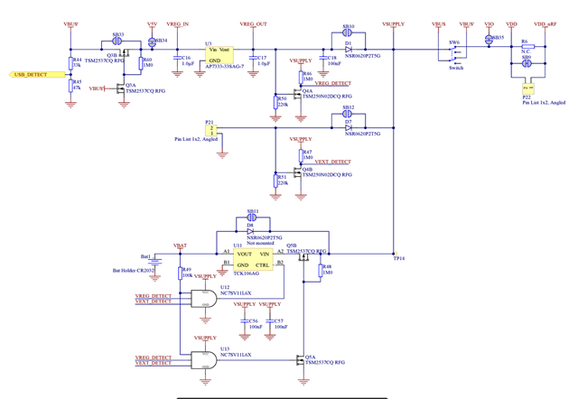
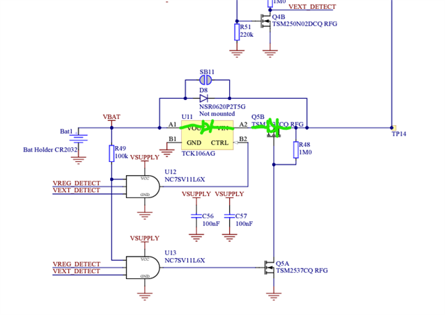
The question is, in the case of no USB power and no External power connected but Coin Cell battery is connected. How would the the battery power go through and load switch?
The AND gates should give 0 and they not even powered! The are supplied by Vsupply and Vsupply should be Zero volts as there is no USB or external power and Coin cell battery is not connected yet to Vsupply!!!
Second question, why you connect the load switch in opposite direction? Normaly, I would expect the battery to be connected to Vin and Vout is connected to Vsupply.
Third, why do you make a load switch and then a MOSFET, is not one enough?
Fourth, Why do you connect the VBUS" through a MOSFET first before the 3.3V regulator?
https://infocenter.nordicsemi.com/pdf/nRF52_DK_User_Guide_v2.x.x.pdf page 11
Thanks,