
Hi Sir/Madam,
What is the maximum allowed voltage at the below 5pins when nRF5340-QKAA is not powered up?
Thanks.
Regards,
Tze Hao
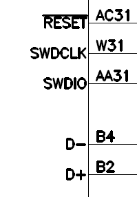
Hi Sir/Madam,
What is the maximum allowed voltage at the below 5pins when nRF5340-QKAA is not powered up?
Thanks.
Regards,
Tze Hao

