Why this L2 and L3 Inductor connected this pin? what is the Purpose of this inductor?
What happen when we not connect?
Why this L2 and L3 Inductor connected this pin? what is the Purpose of this inductor?
What happen when we not connect?
Hi Nikunj,
Thank you for contacting DevZone at NordicSemi.
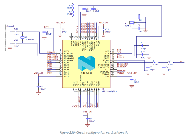
To ensure good RF performance when designing PCBs, it is highly recommended to use the PCB layouts and component values provided by Nordic Semiconductor.
Reference circuits along with components and component values is provided to support on-chip features in a design.
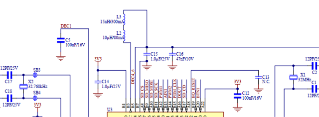
In the nRF52840 reference circuitry, you can see that these inductors (L2 and L3 in series) are connected to the pin DCC of the SoC.
It is shown in "Figure 216: Circuit configuration no. 4 schematic for QIAA aQFN73" of product specification. These are used to support enabling of the DCDC converter.
DCDC feature is enabled for this reference circuitry and the DCC pin is the output of DCDC converter.
Inductors are used to regulate/stabilize current (I) as Capacitors are used to regulate/stabilize voltages (V).
Regards,
Naeem
Thank You so much for your response.
1)Why we connect inductor on DDCH Pin. Inductor value is 10uH in NRF52840-QFAA-F-R
2)When we used SOC in high-impedance mode that time in which pin i get 1v8 ?
Hi Nikunj,
From the product specification document for nRF52840,
As per circuit configuration, high-voltage mode cannot be used
Also, as per reference schematic, there is no need of 10uH inductor that you are mentioning.
Regards,
Naeem
Hi Nikunj,
From the product specification document for nRF52840,
As per circuit configuration, high-voltage mode cannot be used
Also, as per reference schematic, there is no need of 10uH inductor that you are mentioning.
Regards,
Naeem