nRF52810 Flash

Hi,

I have few doubts regarding the internal flash of nRF52810. I am not using SoftDevice. I am using SDK 17.1.0

I would like to write around 20 bytes to internal flash. I would like to use APIs "nrf_nvmc_write_word" and "nrf_nvmc_page_erase" instead of FDS and flash library. The reason is that the write to flash happen rarely and I don't think there is a need of wear levelling in this case. 

  1. How can I know if I am writing to a bad page (write exceeded 10000 cycles) or how can I guarantee that the write is successful ? What will happen if I write to a page of which the cycle has exceeded 10000 ?
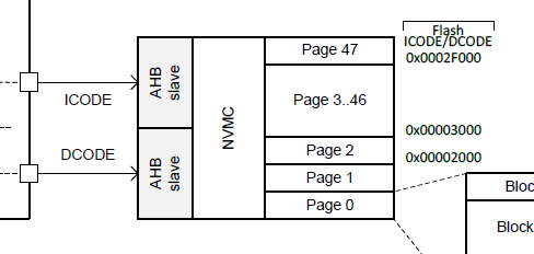
  2. The below given is the block diagram of the internal flash of nRF52810. How can I select the page where I can write my application data ? I know that the internal flash also contain the flashed hex file. How to understand the remaining memory that user can use for his application ?
3. From the below given log from SES,  I understand that the code is flashed to the region 0x0000000 - 0x00001f83. What happens if I try to do a "write" in the code to this region of internal flash ?

4. At what point will be the blocks ".data" and ".bss" will be copied to the ram ? Is it done in the startup code ?

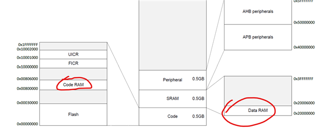
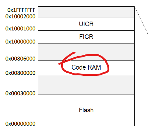
5. What is code RAM ? How is this used ?
  • Hi,

    1. The only way to really find out is to read back what you have just written to see if it matches what you wrote. You may also consider appending a checksum value to your flash data to allow your application to validate the integrity of it if you plan to exceed 10000 write/erase cycles.

    I believe the most typical failure mode for a worn-out flash page is that "random" bits become stuck in one position after an erase or write cycle. 

    2. In practice you can use any page which is not occupied by your FW.  In the Flash Write Example, we use the last flash page.

    3. You will not be prevented from overwriting application code unless you use the BPROT — Block protection peripheral, but it will lead to undefined behavior depending on what you overwrite. 

    4.  Code RAM can be used to execute code from.

    Best regards,

    Vidar

  • Hi Kenneth,

    Thank you for your reply.

    4.  Code RAM can be used to execute code from.

    The datasheet says that nRF52810 has 24 KB RAM, why is it not mentioning 48 KB (data RAM + Code RAM) ?

    Did you mean that there is 48 KB of RAM in total and we can execute the code from "CODE RAM", if needed ? Sorry for the basic questions, but could you please explain the differences ? Are we utilising this space (CODE RAM) in any of the SDK examples ?

  • From the Memory chapter of the PS:

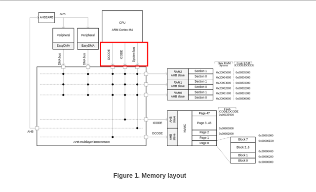
    "The same physical RAM is mapped to both the Data RAM region and the Code RAM region. It is up to the application to partition the RAM within these regions so that one does not corrupt the other."

    In other words, the code RAM and the data RAM are both pointing to the same 24K of RAM in HW. The difference is which memory bus the CPU will use to access it. Data ram is on the System Bus, while code RAM is on DCODE and IDCODE:

    It is possible to execute code from Data RAM as well, but it will introduce wait states and have a negative impact on the performance (worse than FLASH).

Related