ANT pin maximum work voltage @ 6.78MHz

Hi,

The antenna we use with the nRF52832 for BLE comm. is also exposed to high radiation at the 6.78MHz band simultaneously.

We can use countermeasures in order to block the 6.78MHz induced voltage from reaching the nRF52832 ANT pin but need to design them using a target value.

What is the maximum voltage allowed at the ANT pin @ 6.78MHz in order to maintain an undegraded BLE comm.?

What is the absolute maximum voltage at the ANT pin @ 6.78MHz? Is there a recovery time for maintaining an undegraded BLE comm.?

Can you share with us a detailed internal RF diagram?

Thanks,

Amiel

  • Max power on the ANT pin is 10 mW without damage. In 50 ohm, this is 0.7 Vrms. 

    The matching network on the ANT pin acts as a low pass filter and will not attenuate lower frequency signals. A simple high pass filter before the antenna will attenuate the 6.78 MHz signal. The attenuation depends on the strength of the signal. Approximately how much are we talking about here?

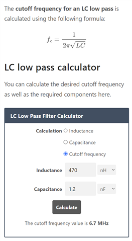
    You could also use a series resonance filter https://www.allaboutcircuits.com/textbook/alternating-current/chpt-6/simple-series-resonance/ This is easier to mount on the existing design to test as it's only two components in series to ground. For instance


  • Thanks ketiljo.

    I guess the ANT port impedance is different from 50 Ohm @ 6.78MHz thus requested the voltage level since power alone does not help here especially if the ANT port is very reactive @ 6.78MHz.

    I actually intend to use a series RLC notch filter parallel to the ANT line, resonating @ 6.78MHz, to form a narrow band reject filter. Does a wide band S1P of the ANT port that covers the 6.78MHz band is available?

    The current line up we use attenuates the 6.78MHz signal to 2-4 hundreds of mVptp on the ANT pin. My concern is that potentially there will be orders of magnitude between the BLE Rx (wanted) signal and the 6.78MHz (unwanted) signal while i don't know anything about the selectivity @ 6.78MHz nor the impact on PER (or other qualitative comm. parameter) in this situation. it might be a situation of uV at the BLE band and mV at the 6.78MHz band.

    I appreciate your effort in replying my question.

  • The RX shouldn't be affected much by the signal if it's only a few hundred mV. A LC notch should be enough here. It's so far from the operating frequency and the internal balun, LNA filter and matching takes care of this. I'm more worried about the TX where signal can be modulated onto the carrier and show up as side band spurious. You can test this quite easily if you setup a constant carrier and measure the spectrum.

  • Hi, I assumed there is a rejection in the 6.78MHz band but i looked for data that will help quantify a target amplitude value for not degrading the BLE comm. quality through saturation or IMDs of BLE+6.78MHz from one hand when they are both strong or through spurs/blocking relating to the 6.78MHz when the BLE is much weaker. Both in reception.

    That is how i can design the rejection of the link to 6.78MHz energy and also have a number to work with.

    Since i don't know the front end structure i can't tell what happens if the 6.78MHz goes through the TR switch, would it pass the output matching of the PA and mix? I don't know, but that's a good idea to test it.

    Thank you very much.

  • The ANT pin is directly connected to a balun with the other end grounded. The energy transfer through this to the T/R switch and the LNA should be pretty low. If the field is strong enough I guess anything can happen. I think the best is just to test this. You could do this with a DK and mount the LC notch near the connector to the antenna. 

Related