RTC causes VDD to rise in deep sleep mode

I have some custom hardware that uses an nRF52832 interfaced to a PCF85063A RTC.  I'm using I2C0 to communicate with the RTC, and am coding with v2.2.0 of NCS.

My MCU spends most of its time in deep sleep, occasionally exiting when triggered by a GPIO.  It then grabs the date and time from the RTC, logs some info, and then goes back into deep sleep.

Problem I am seeing is that at this point, the VDD rail seems to mysteriously "charge" up from 3.0V to around 6V, where it will remain until I trigger the MCU out of deep sleep again.

I've tracked this issue down to the RTC itself - I have a bunch of other GPIO that I disconnected, but this didn't change the situation.  Things only improved when I disconnected the two 4K7 pull up resistors on the SCL (P0.27) and SDA (P0.26) lines.

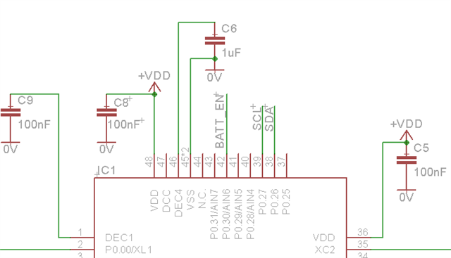
This is how things are configured in hardware:


And this is what I am seeing if I monitor VDD on my scope.  VDD is charging up from 3V to 6V over about 1 sec.  I have about 10uF of capacitance in total across my VDD.

I can fix this issue by putting a 47K resistor across VDD, but that defeats the purpose of having the MCU in deep sleep, as it means I go from a ~ 500nA current to > 50uA sleep current.

Is there something I should be doing with the I2C0 port prior to going into deep sleep to prevent this from happening?

Cheers,

Mike

Parents
  • Where does VDD come from? Is there a series LDO or DC-DC or battery? There may be an issue with minimum current, in that this may be simple leakage although disconnecting 4k7 pull-ups indicates a voltage doubler effect; however unless the nRF52 GND is faulty 6V will cause failure of the nRF52 in any case which implies the nRF52 is not correctly connected to the common GND (ie a GND break between nRF52 and regulator or clock)

  • I'm generating VDD (3V) via a 9V battery and a LDO linear regulator (using the TPS77030 as its got the lowest quiescent and ground currents of any LDO I could find).  See screen shot of the relevant section of the schematic below.  Note that R20/R21/R9/R10/Q2 are used for measuring battery voltage.

    I did test the DC-DC conversion stage in isolation, with just a resistive load that I would apply to simulate "on" mode, and then removed that load to simulate deep sleep (so, in this mode, the LDO had zero load).  The LDO was able to keep regulation with no issue, so I know its not an issue with that.

    I'm guessing the nRF52 or my RTC has some sort of internal ESD protection that is limiting the rise on VDD to 6V, and because there is very little current behind that voltage source, its not actually causing any damage to the MCU.  But its not something I want to be seeing in my production version, hence why I'm trying to sort this issue out.

    I can verify that there is GND continuity across my board - I have a 4 layer board, with:

    • the bottom layer and Layer 2 acting as a GND plane
    • layer 3 as the power (VDD) plane
    • top layer as the signal layer

    In terms of how I've connected my nRF52 to VDD and GND, I've followed a very similar approach to that used on the nRF52-DK.

    Looking at the specs for the nRF52, it mentions something about configuring the SCL/SDA pins prior to going into low power mode

    I am wondering if this has something to do with the issue I am seeing

    Mike

Reply
  • I'm generating VDD (3V) via a 9V battery and a LDO linear regulator (using the TPS77030 as its got the lowest quiescent and ground currents of any LDO I could find).  See screen shot of the relevant section of the schematic below.  Note that R20/R21/R9/R10/Q2 are used for measuring battery voltage.

    I did test the DC-DC conversion stage in isolation, with just a resistive load that I would apply to simulate "on" mode, and then removed that load to simulate deep sleep (so, in this mode, the LDO had zero load).  The LDO was able to keep regulation with no issue, so I know its not an issue with that.

    I'm guessing the nRF52 or my RTC has some sort of internal ESD protection that is limiting the rise on VDD to 6V, and because there is very little current behind that voltage source, its not actually causing any damage to the MCU.  But its not something I want to be seeing in my production version, hence why I'm trying to sort this issue out.

    I can verify that there is GND continuity across my board - I have a 4 layer board, with:

    • the bottom layer and Layer 2 acting as a GND plane
    • layer 3 as the power (VDD) plane
    • top layer as the signal layer

    In terms of how I've connected my nRF52 to VDD and GND, I've followed a very similar approach to that used on the nRF52-DK.

    Looking at the specs for the nRF52, it mentions something about configuring the SCL/SDA pins prior to going into low power mode

    I am wondering if this has something to do with the issue I am seeing

    Mike

Children
Related