Hi there,
I'm trying to implement "poor man's gang programmer" in the following way -
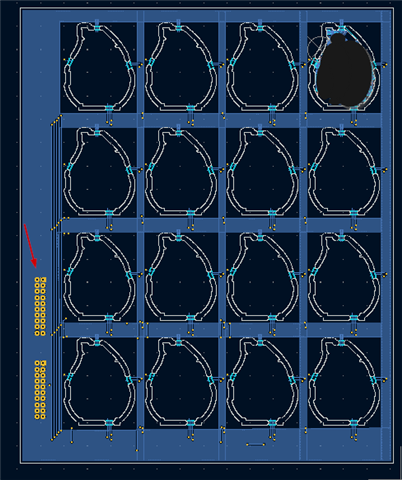
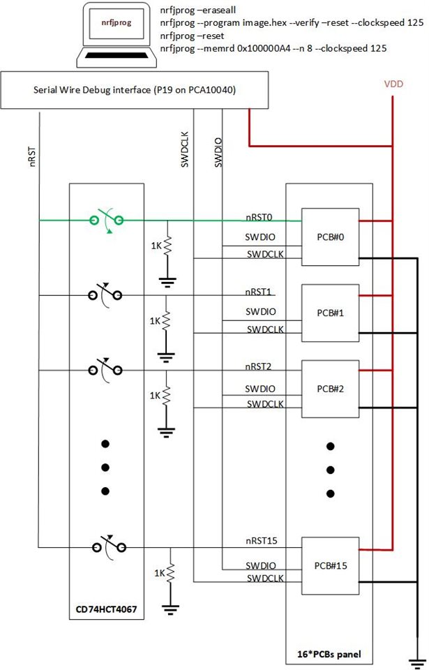
- On the edge of a 16 PCBs panel, there's a 2*10 pins row easily accessed by 2*10 pogo pin adapter
- The signals in this header are:
- 16*nRST signals, one for each PCB
- SWDIO & SWDCLK shared between all PCBs
- VDD & GND
- The 16 nRST signals are designed so 15 of them are grounded and one is routed to the nRST signal of the SWD programmer (see attachged drawing)
Currently, while testing, 15 are hard-grounded and one is hard-wired to nRST of the programmer.
In the production setup, all 16 will be routed through an analog switch. 15 will be pulled down (1K) and one will be connected directly - I'm using PCA10040 SWD for testing and nrfjprog as a command line tool.
The commands I play with are:
nrfjprog –eraseall
nrfjprog --program image.hex --verify –reset --clockspeed 125
nrfjprog –reset
nrfjprog --memrd 0x100000A4 --n 8 --clockspeed 125

I fail to achieve a stable performance, most of the time I get any of the following nrfjprog error messages:
- [error] [SeggerBackend] - 10 second timeout elapsed, no time left to wait for debug port to power up.
Failed to read device memories.[error] [SeggerBackend] - 10 second timeout elapsed, no time left to wait for debug port to power up.
OR - [error] [SeggerBackend] - JLinkARM.dll reported "-1", "An unknown error.".
[error] [SeggerBackend] - JLinkARM.dll reported "-1", "An unknown error.".
[error] [SeggerBackend] - JLinkARM.dll reported "-1", "An unknown error.".
[error] [SeggerBackend] - JLinkARM.dll reported "-1", "An unknown error.".
[error] [SeggerBackend] - JLinkARM.dll reported "-1", "An unknown error.".
[error] [ nRF52] - The write access failed, but no cause could be determined.
[error] [ nRF52] - It may be due to an unaligned access, accessing a nonexistent memory, or a communication issue.
[error] [ nRF52] - Failed writing to code!
[error] [ nRF52] - Failed to program flash
[error] [ nRF52] - Failed while programming file Tempdrop2-image.hex.
ERROR: JLinkARM DLL reported an error. Try again. If error condition
ERROR: persists, run the same command again with argument --log, contact Nordic
ERROR: Semiconductor and provide the generated log.log file to them.
NOTE: For additional output, try running again with logging enabled (--log).
NOTE: Any generated log error messages will be displayed.
OR - [error] [SeggerBackend] - 10 second timeout elapsed, no time left to wait for debug port to power up.
Failed to read device memories.
[error] [SeggerBackend] - 10 second timeout elapsed, no time left to wait for debug port to power up.
[error] [ nRF52] - Failed when checking readback protect status.
ERROR: Operation failed due to timeout. Check the log messages for more details.
NOTE: For additional output, try running again with logging enabled (--log).
NOTE: Any generated log error messages will be displayed.
I've noticed in the specifications that swdclk & swdio pins have an internal pull-up. That means that, as these lines are shared, the equivalent pullup the programmer sees is Rpu/16.
Can this explain my problems?
Is there a way to recover this mass-programming concept?
Many thanks.