How to read a frame from hm01b0 image sensor?

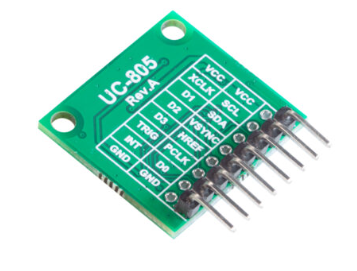
I am attempting to connect the Arducam hm01b0 to the nRF52840-DK embedded board, utilizing bare metal programming. The sensor comes with the following pins for serial interface. To access 4-bit interface( D1,D2,D3 and D4), the user has to solder the pins. However I am trying to get the HM01B0 working over the 1-bit interface and try to capture an image.
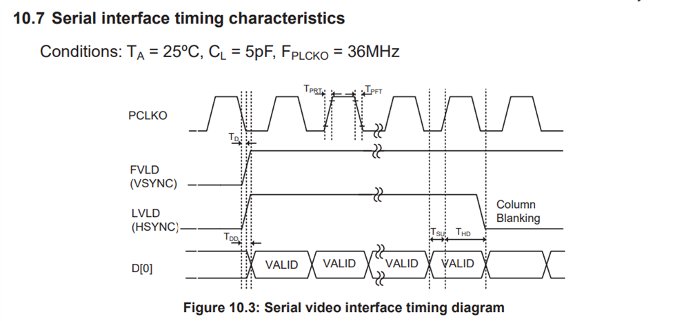
I am able to read and write to the sensor registers over I2C. The datasheet presents the following timings characteristics to capture an image.
I have connected the logic analyzer and I am able to see the corresponding waveform that is the data is being streamed over D0 line.

For 1 bit interface,the image sensor has a frame rate of 30 FPS and the frequency of PCLK is 36 Mhz. I know that GPIO pins would not be able to read the input signals in this

frequency range but I don't know how else to read a serial line. One option is making the image sensor as SPIM master and nrf52840 as SPIM slave. The image sensor provides the clock over PCLK which can be configured as SPI clock and the line D0 can be configured as MOSI line. However to read valid data bits/bytes over the serial line, VSYNC and HSYNC should also be read and made sure that their value is according to the serial video interface timings diagram. So I tried to read the serial line D0 by configuring it as a GPIO pin and I read 0x00 always.

How can I configure the image sensor and capture an image? 

This is the code I have written,

// array to hold a complete frame
uint8_t  frameBuffer[324][324];

#define PIN_VSYNC      (28)          
#define PIN_HSYNC      (29)          
#define PIN_PCLK       (30)
#define PIN_D0         (31)     

// initialise the pins of sensor
void hm0360_init()
{
    // GPIO I/P
    nrf_gpio_cfg_input(PIN_VSYNC, NRF_GPIO_PIN_PULLUP);
    nrf_gpio_cfg_input(PIN_HSYNC, NRF_GPIO_PIN_PULLUP);
    nrf_gpio_cfg_input(PIN_PCLK, NRF_GPIO_PIN_PULLUP);

    // GPIO O/P
     nrf_gpio_cfg_input(PIN_D0,NRF_GPIO_PIN_PULLUP);


    for(int i = 0; i < 324 ; i++){
        for(int j = 0; j < 324 ; j++){
            frameBuffer[i][j] = 0;
        }
     }
}


void hm01b0_read_frame_bits()
{
   int VSYNC_count = -1, HREF_count = 0;
   int incomingBits;
    unsigned char byte = 0;
    int byteArrayIndex = 0;
    int bitCount = 0; 

while(nrf_gpio_pin_read(PIN_VSYNC) == LOW) { }
while(nrf_gpio_pin_read(PIN_VSYNC) == HIGH)
{
	while(nrf_gpio_pin_read(PIN_HSYNC) == false && nrf_gpio_pin_read(PIN_VSYNC) == HIGH) { }
    VSYNC_count++;
	HREF_count = 0;
	//Read a row
	while(nrf_gpio_pin_read(PIN_HSYNC) == true) 
	{ 
		while(nrf_gpio_pin_read(PIN_PCLK) == false) { }
		// read 0 always
		incomingBits = nrf_gpio_pin_read(PIN_D0);
		byte = (byte << 1) | incomingBits;
		bitCount++;

		if (bitCount == 8) {
			frameBuffer[VSYNC_count][HREF_count++] = byte;
			bitCount = 0;
			byte = 0;
		}

		if (VSYNC_count == 324) {
			break;
		}
		
		while(nrf_gpio_pin_read(PIN_PCLK) == true) { }
	}
	
}

}

You can find the datasheet of the image sensor here : www.uctronics.com/.../HM01B0-MWA-image-sensor-datasheet.pdf

Parents
  • I am attempting to do the same thing. I know it is possible because it was documented in a Science Robotics article in 2020. Here is some information that will hopefully help everyone (pp. 5):

    To allow the Bluetooth chip to read the image sensor data directly at the highest frame rate requires a direct memory access (DMA) feature. The DMA feature, however, is only exposed for certain common communication protocols, none of which are supported by the camera. The camera only outputs data and clock signals. To read the camera data, we repurposed the serial peripheral interface (SPI) interface, which does have access to DMA. Reading data over the SPI interface requires a data signal, a clock signal, and a chip select (CS) signal. We could directly use the camera’s data and clock outputs for the first two. However, to provide the missing CS signal required by the protocol, we leveraged the line-valid output of the camera. This signal was configured to trigger an interrupt on the Bluetooth chip, which toggles an output pin to spoof the missing CS signal.


    This will be my first project with the NRF52832. I don't really know where to start. Probably with some simpler practice problems?

  • As a hint I may advise you to use GPIOTE to invert the HSYNC and use that as CS line for SPI Slave interface (SPIS):

        nRF52 SPIS interface CS signal must be on external physical pin, cannot be triggered internally.
         Polarity of CS line is also not negotiable.
        Considering above, we have to 'waste' 2 additional pins to do the inversion job.

    //One pin is for monitoring the HSYNC line from camera

    #define GPIOTE_CONFIG_IN_SYNC \
    { \
    .is_watcher = false, \
    .hi_accuracy = true, \
    .pull = NRF_GPIO_PIN_PULLDOWN, \
    .sense = NRF_GPIOTE_POLARITY_TOGGLE, \


    //Second pin is used as dummy CS_OUT line . Inversion is done using PPI:
     
    nrf_drv_gpiote_in_config_t config1 = GPIOTE_CONFIG_IN_SYNC;
    nrf_drv_gpiote_out_config_t config2 = GPIOTE_CONFIG_OUT_TASK_TOGGLE(true); //init high to inverse
    err_code = nrf_drv_gpiote_out_init( DUMMY_CS_OUT, &config2);
    APP_ERROR_CHECK(err_code);

    nrf_drv_gpiote_out_task_enable(DUMMY_CS_OUT);

    err_code = nrf_drv_gpiote_in_init(HM01B0_HSYNC, &config1, NULL); //null: no interrupt 
    APP_ERROR_CHECK(err_code);
    nrf_drv_gpiote_in_event_enable(HM01B0_HSYNC, false); // no INT
    err_code = nrf_drv_ppi_channel_assign( ppi_channel_spi_start,
    nrf_drv_gpiote_in_event_addr_get(HM01B0_HSYNC),
    nrf_drv_gpiote_out_task_addr_get(DUMMY_CS_OUT) );
    APP_ERROR_CHECK(err_code);

    //The DUMMY_CS_OUT is connected physically to the 3rd pin used: line declared as CS_IN in SPIS parameters.

    Cheers
    TKa

Reply
  • As a hint I may advise you to use GPIOTE to invert the HSYNC and use that as CS line for SPI Slave interface (SPIS):

        nRF52 SPIS interface CS signal must be on external physical pin, cannot be triggered internally.
         Polarity of CS line is also not negotiable.
        Considering above, we have to 'waste' 2 additional pins to do the inversion job.

    //One pin is for monitoring the HSYNC line from camera

    #define GPIOTE_CONFIG_IN_SYNC \
    { \
    .is_watcher = false, \
    .hi_accuracy = true, \
    .pull = NRF_GPIO_PIN_PULLDOWN, \
    .sense = NRF_GPIOTE_POLARITY_TOGGLE, \


    //Second pin is used as dummy CS_OUT line . Inversion is done using PPI:
     
    nrf_drv_gpiote_in_config_t config1 = GPIOTE_CONFIG_IN_SYNC;
    nrf_drv_gpiote_out_config_t config2 = GPIOTE_CONFIG_OUT_TASK_TOGGLE(true); //init high to inverse
    err_code = nrf_drv_gpiote_out_init( DUMMY_CS_OUT, &config2);
    APP_ERROR_CHECK(err_code);

    nrf_drv_gpiote_out_task_enable(DUMMY_CS_OUT);

    err_code = nrf_drv_gpiote_in_init(HM01B0_HSYNC, &config1, NULL); //null: no interrupt 
    APP_ERROR_CHECK(err_code);
    nrf_drv_gpiote_in_event_enable(HM01B0_HSYNC, false); // no INT
    err_code = nrf_drv_ppi_channel_assign( ppi_channel_spi_start,
    nrf_drv_gpiote_in_event_addr_get(HM01B0_HSYNC),
    nrf_drv_gpiote_out_task_addr_get(DUMMY_CS_OUT) );
    APP_ERROR_CHECK(err_code);

    //The DUMMY_CS_OUT is connected physically to the 3rd pin used: line declared as CS_IN in SPIS parameters.

    Cheers
    TKa

Children
No Data
Related