Programming with nRF52833DK with SWD at 1.8V

Hello!

I have been developing with the nRF52833, and have built a custom PCB to interface with an on board nRF52833 SoC.

The PCB has VDDH connected separately to 3.3V and, by default, VDD will operate at 1.8V (VDDH and VDD are not shorted so we are in High voltage mode)

The plan was to use the nRF52833 DK to program the custom board. The pin setup is as follows:

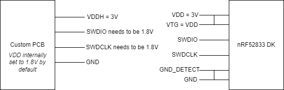
SWD is dependent on VDD, therefore SWDIO and SWDCLK need to be at 1.8V. However, the dev board provides it at 3V.

I am using P20 on the development kit with VTG tied to VDD and GND_Detect tied to GND.

To solve this I have tried the following:

1. VDD = 3V, SWDIO/SWDCLK are level shifted down using MOSFETs

2. VDD = 3V, SWDIO/SWDCLK are divided using a resistor network to 1.8V

3. Toggle SW9 so VDD is not dependent on USB and we can still use USB to program. Power VDD on dev board externally with 1.8V. Then step up VDD to 3.3V (op-amp) before sending that to PCB (on VDDH). SWD interfaces should be at 1.8V

None of these approaches have worked so far. I would have thought level shifting would have worked, but maybe there is something about the SWD interface which prevents this. OR I shouldn't use MOSFET level shifting and there's a better method. Either way, I feel like it's possible to still program the custom board even with this setback. Hoping someone here can provide more assistance!

Thanks!

Parents
  • Hi

    Our Development kits are only designed for programming external targets at 3.0V VDD, and we would recommend one of the J-Link devices that officially support programming at the voltage you need. However, a note in the DK user guide (page 32) says "The voltage supported by external debugging/programming is VDD voltage. Normally, this is 3 V when running from USB, but if the onboard nRF52833 SoC is supplied from either USB or Li-Ion, the nRF power source switch (SW9) is in either Li-Po or USB position," VDD can be set to other voltages. "For both P19 and P20, the interface MCU will detect the supply voltage on the mounted shield and program/debug the target." However, it is not designed for or tested for programming at other voltages, but it might work.

    Best regards,

    Simon

Reply
  • Hi

    Our Development kits are only designed for programming external targets at 3.0V VDD, and we would recommend one of the J-Link devices that officially support programming at the voltage you need. However, a note in the DK user guide (page 32) says "The voltage supported by external debugging/programming is VDD voltage. Normally, this is 3 V when running from USB, but if the onboard nRF52833 SoC is supplied from either USB or Li-Ion, the nRF power source switch (SW9) is in either Li-Po or USB position," VDD can be set to other voltages. "For both P19 and P20, the interface MCU will detect the supply voltage on the mounted shield and program/debug the target." However, it is not designed for or tested for programming at other voltages, but it might work.

    Best regards,

    Simon

Children
  • Hi Simon,

    Thanks for the response!

    I do have access to a pad, so I can temporarily bypass VDDH logic and have VDD at 3V. I was able to program this way. I'm thinking of then modifying the REGOUT0 value (with nrfjprog) to set it at 3V so I no longer have to touch the pad and can still use the development board to program the PCB.

    Long term I'll redesign to make everything 3V again. Appreciate the support!

Related