SPI Master can't work together with bluetooth stack

Hello Nordic,

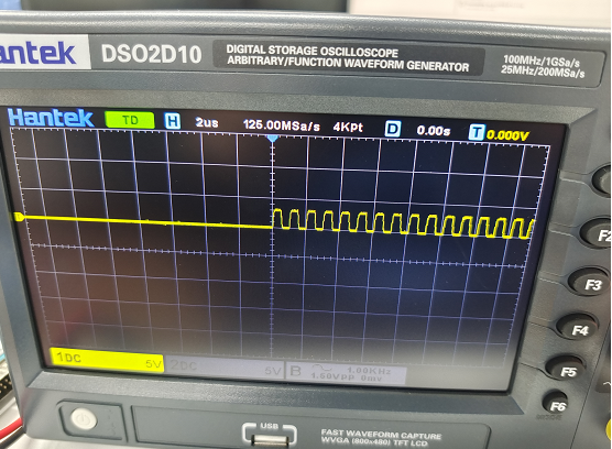
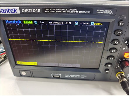
I want to use SPI master with bluetooth on nrf52840 board. When I use the project under nRF5_SDK_17.1.0\examples\peripheral\spi, I can see the clock signal under oscilloscope. But when I add the SPI master code into the project of nRF5_SDK_17.1.0\examples\ble_peripheral\ble_app_uart. I can not see clock signal under oscilloscope. And I notice that the SPI master is blank project, and the bluetooth is s140 project. Can you give me any suggestion about this problem?
Parents
  • Hi,

    Can you post the code where you have integrated SPI with ble_app_uart?

    Do you start the transfer(s) from main or interrupt context?

    Which GPIOs are you using for MOSI and MISO?

    Is the other parts of the application working as expected?

    Do you run this on a nRF52840 DK, or on a custom board?

    Best regards,
    Jørgen

  • It seems you are passing wrong length parameters to nrf_drv_spi_transfer(). If your intention is to write 1 or 2 bytes, then read out 1 byte after writing is done, you need to set the rx_length parameter to tx_length + rx_length. The RX buffer will start filling when you clock out data from TX buffer, and will stop when you reach the specified rx_length. The function will not first do TX and then do RX after this, as some SPI devices may support full duplex write/read operations (write address for next read while you read out data from last write, etc).

    AllenSun said:
    But I always read the data is 0x00, even though no MISO and MOSI connected

    If the pins are not connected, why do you expect different values?

  • Jorgen, Thank you for your reply. But it still does not work, even if I set rx_length as you said. Both m_rx_buf[0]  and m_rx_buf[1] are 0x00. Do you have sample code of Nrf52840 write/read Ads1293 correctly? 

    static uint8_t ads1293_read_reg(uint8_t addr)
    {
    uint8_t value = 0;

    nrf_gpio_pin_clear(ADS1293_SS);

    user_spi_wdata(ADS1293_READ_BIT | addr);

    value = user_spi_rdata(0x00);

    nrf_gpio_pin_set(ADS1293_SS);

    return value;
    }

    static uint8_t user_spi_rdata(uint8_t data)
    {
    spi_xfer_done = false;

    m_tx_buf[0] = data;
    m_rx_buf[0] = 0xff;
    m_rx_buf[1] = 0xff;

    APP_ERROR_CHECK(nrf_drv_spi_transfer(&spi, m_tx_buf, 1, m_rx_buf, 2));

    while (!spi_xfer_done)
    {
    __WFE();
    }

    if(m_rx_buf[0] == 0){printf("0x%x", m_rx_buf[0]);}
    if(m_rx_buf[1] == 0){printf("0x%x", m_rx_buf[1]);}

    return m_rx_buf[1];
    }


  • If you set the rx_buf to 0xFF before transfer and it is set to 0x00 after transfer, the MISO line is likely not toggled during the transfer. Again, which pins are you using for SCK/MISO/MOSI/SS? Have you checked the pins with a logic analyzer/scope to see if all toggle as expected?

Reply Children
No Data
Related