
Hi all,
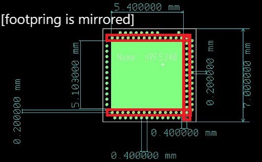
I'm developing a custom board based on the nRF5340 chip and I'm having trouble routing the traces for the inner SMD pads in the QFN package. I believe that the reference layout uses via-in-pad for the inner pads to avoid the issue of top layer traces conflicting with the outer pads. However, after talking to a lot of circuit board manufacturers, a via-in-pad design will be extremely difficult to manufacture due to how small the nRF5340 QFN pads really are.
The pad size is around .2mm, meaning the via pad will need to be no larger than .2mm (~7 mil). This leaves either:
a) Extremely small via drill size (under 4 mil) or
b) Extremely small via annular ring
Either way, there were doubts that my design would be manufacturable. Does anyone have advice for routing traces using very small vias-in-pads or another creative method? I'm open to all options for routing traces to the inner pads!
(Using Ultiboard if that matters)
Thank you,
Nick B

