Hello,
We are using nRF9160 for asset tracking product. We used nRF52832 as an BLE+MCU. I have some queries regarding the schematic design of nRF9160.
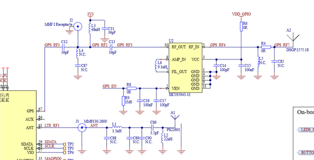
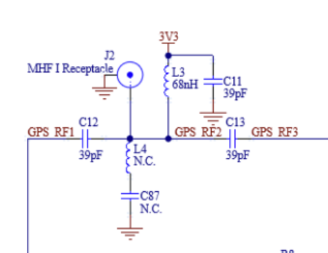
1. Is it mandatory to use LNA and Antenna tuner circuitry for GPS antenna? or I can just go with T or Pi matching circuitry?
2. What is the purpose of COEX pins? We are using the BLE of nRF52832 and using nRF9160 for GPS and NB-IoT connectivity. Is it mandatory to use or I can let them unconnected?
We are sending GPS data to nRF52832 after every 30 mins and we required minimum current consumption for continues tracking.
3. In datasheet it is written in VDD_GPIO recommendation :
VDD_GPIO should be applied after VDD has been supplied
VDD_GPIO should be removed before removing VDD
I am not sure how to design the circuit with above requirements.
4. Please guide me to make RESET pin circuit as weel because I am bit confuse after seeing nRF9160 DK RESET circuit.