Schematic review

Good morning, 
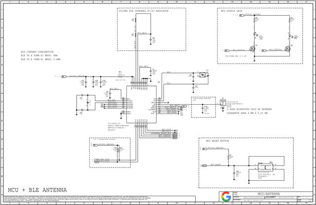
I ended up changing the design to use the nRF52810 chipset and I wanted to find out if Nordic would be able to provide some schematic feedback for my design. Below is the schematic: 
I have a couple of questions I wanted clarified: 
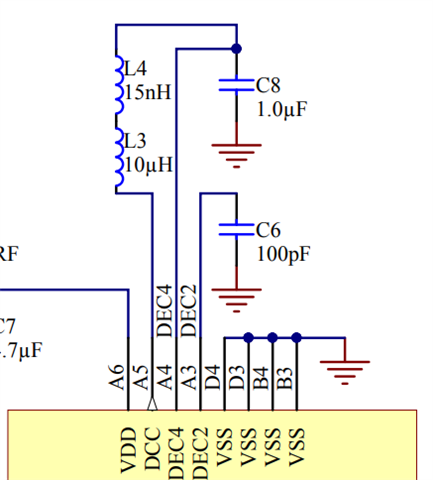
1. On the reference design you have a 10uH and a 15nH inductor in series for the DC/DC regulator filter. Is the 15nH inductor necessary? 
2. I have used the following xtal crystals for the 32.768Hz and the 32MHz frequencies respectively: 9H03280012, and 8Q32070006. Will these work well for your chipset? Also recommended known ones you have used in the past if these don't work. 
3. I am using this chip antenna on the board, let me know if you foresee any issues with this: w3008
Looking forward to hearing from you. 
Many thanks 
Tinashe
Google
  • You may you viewmate viewer, which is free to download to look at the ODB++ file in case your default viewer doesn't work

  • Hello,

    I have checked the design.

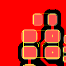
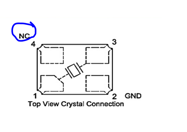
    The pin 4 of the high frequency crystal is not grounded. You can see pin 4 is floating. 

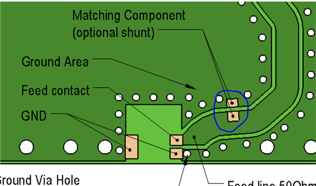
    You do not have any antenna matching network in the design. Based on your antenna matching network would vary. You can look into these issues.

    Thanks.

    BR

    Kazi

  • Hi Kazi, 

    Thanks for the feedback. 

    Pin 4 is supposed to be floating. 

    Antenna matching is optional. The antenna input impedance is 50 ohm. 

    Thanks 

  • Hi Tinashe,

    So for the Crystals, we often recommend to ground even the NC pin, it is not necessary. Reason for this is that we have seen some cases where customers has mounted the crystals with a 180 degree rotation. And as far as i am aware we have not seen any down sides by grounding the NC pin. 

    But feel free to do as the datasheet recommend, as that is the actual recommendation of the components that you are using.


    tmarera said:
    Antenna matching is optional. The antenna input impedance is 50 ohm.

    It often says optional in the datasheets of these chip antennas, but more often then not there needs to be some tuning. This is due to the fact that there are other factors that is effecting the antenna, like the casing of the product and in what environment it is mounted.

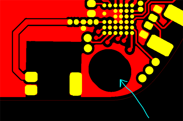
    I like to recommend a full Pi-network as close to the antenna as possible. And since you do in fact have a large hole right next to the antenna, probably for the mounting mechanism of the PCB, it can\will effect the antenna, so it is likely that some tuning is needed for optimal performance.


    I also see that the files in the .tgz does not match the images you uploaded first, did you do some changes,what is the latest versions?


    Adding some general comments on the layout here:


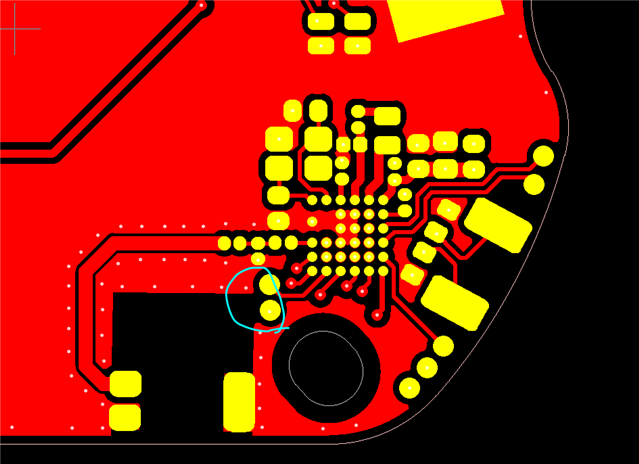
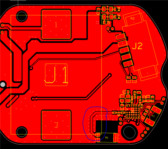
    The ground area on the top layer around the antenna should ideally be a consecutive layer, so try to tie the two sections of top layer GND together.

    There seems to be enough room to move the SoC and the components further in that would give you more room to have a consecutive plane around the antenna.


    I am curious about the J1, how large is it an will it cover parts of the antenna or the transmission line? This could effect the impedance of the trace.


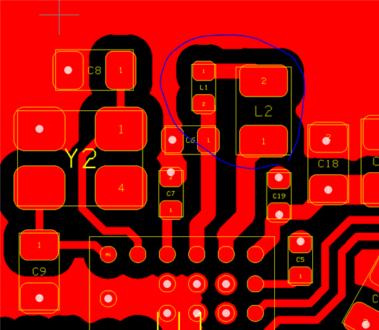
    L1 and L2 should not be placed orienting the same way, the inductors have a chance of resonating so to minimize the risk one of the inductors should be rotated 90 degrees.


    Regards,
    Jonathan

Related