Matching Network Placement and Routing-BLE Antenna Routing

Dear Nordic Team,

Please help me clear a query as we know we must maintain the 50ohm impedance in the RF Track.
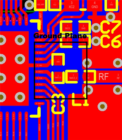
Someone suggests I maintain the ground clearance between the 1st Component of the Matching network as shown in the image-

If we did this as per my knowledge we could not maintain the 50 Ohm Impedance(if we provide clearance for C3 GND Pin). Please correct me if I am wrong.


Please feel free to contact me in case of any queries.


Thanks & Regard
Syed Afzal

Hardware Design Engineer 
Atlanta Systems Pvt. Ltd
M-135 2nd Floor, Connaught Place
New Delhi-110001
Mob- +917503601370 |  http://www.atlantasys.com


Parents
  • Hi,

    The ANT pin is not 50Ohm so looking from L1 and in to the ANT pin we don't need it to be 50 Ohm's. But out from the L1 and towards the antenna then the transmission line should maintain 50 Ohm's. 

    Illustration:


    Regards,
    Jonathan

  • Hey Jonathan,

    Thanks for your response.


    Please also confirm that the recommended image as shown is based on nrf52832. Right!

    ->I will remember it for further Design but also clarify my point for C3 we have to provide the ground plane clearance or not as shown in the image below-
     

    -> Also please clear one more query related to nRF52833. We have to do the same procedure in clearance for the nRF52833

    After L2 we have to add a Pi network and maintain a 50-ohm impedance. Right!


    Thanks & Regard
    Syed Afzal

    Hardware Design Engineer 
    Atlanta Systems Pvt. Ltd
    M-135 2nd Floor, Connaught Place
    New Delhi-110001
    Mob- +917503601370 |  http://www.atlantasys.com


  • Afzal said:
    Please also confirm that the recommended image as shown is based on nrf52832. Right!

    Correct, but there is some modifications, removed some components on other pins for less visual clutter.  We do have some guides on HW design here here  https://devzone.nordicsemi.com/guides/short-range-guides/b/hardware-and-layout/posts/nrf52832-specific-pcb-guidelines  and here https://devzone.nordicsemi.com/guides/short-range-guides/b/hardware-and-layout/posts/general-pcb-design-guidelines-for-nrf52

    Afzal said:
    clarify my point for C3 we have to provide the ground plane clearance or not as shown in the image below-

    There are two reasons to why the layout is at it is. Firstly it serves as the matching to get to 50 Ohms, and secondly it serves as a filter for harmonics. So the specific layout helps suppress the unwanted harmonics. 

    So we highly recommend that you include the keep out zone/ground plane cleared area on the top layer for best performance. 

    Afzal said:
    Also please clear one more query related to nRF52833. We have to do the same procedure in clearance for the nRF52833

    Yes, also follow the layout example we have here for best performance. 


    Afzal said:
    After L2 we have to add a Pi network and maintain a 50-ohm impedance. Right!

    The Pi network is just an example of what can be used for properly matching the antenna. A T or some other network is also perfectly fine, and if you are using a specific antenna that has some recommendations in terms of matching components then use that. But we see that in most cases the typical Pi network placed close to the antenna works great. 


    PS:
    We do schematic and hardware reviews so if you want to have your design review we can do that, all you need to do is create a new Devzone ticket either private or public and name it HW review. 

Reply
  • Afzal said:
    Please also confirm that the recommended image as shown is based on nrf52832. Right!

    Correct, but there is some modifications, removed some components on other pins for less visual clutter.  We do have some guides on HW design here here  https://devzone.nordicsemi.com/guides/short-range-guides/b/hardware-and-layout/posts/nrf52832-specific-pcb-guidelines  and here https://devzone.nordicsemi.com/guides/short-range-guides/b/hardware-and-layout/posts/general-pcb-design-guidelines-for-nrf52

    Afzal said:
    clarify my point for C3 we have to provide the ground plane clearance or not as shown in the image below-

    There are two reasons to why the layout is at it is. Firstly it serves as the matching to get to 50 Ohms, and secondly it serves as a filter for harmonics. So the specific layout helps suppress the unwanted harmonics. 

    So we highly recommend that you include the keep out zone/ground plane cleared area on the top layer for best performance. 

    Afzal said:
    Also please clear one more query related to nRF52833. We have to do the same procedure in clearance for the nRF52833

    Yes, also follow the layout example we have here for best performance. 


    Afzal said:
    After L2 we have to add a Pi network and maintain a 50-ohm impedance. Right!

    The Pi network is just an example of what can be used for properly matching the antenna. A T or some other network is also perfectly fine, and if you are using a specific antenna that has some recommendations in terms of matching components then use that. But we see that in most cases the typical Pi network placed close to the antenna works great. 


    PS:
    We do schematic and hardware reviews so if you want to have your design review we can do that, all you need to do is create a new Devzone ticket either private or public and name it HW review. 

Children
Related