Understanding Power Supply + SWD target voltage

Hey!

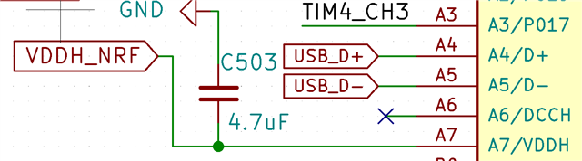
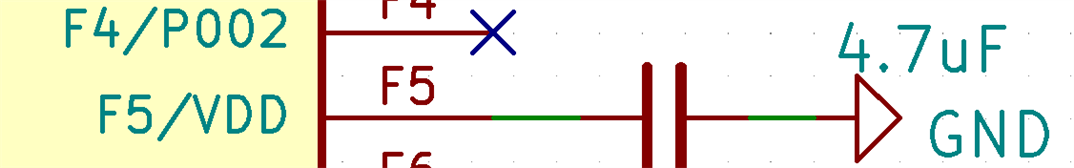
I designed and fabricated a PCB using the NRF52840, but I'm encountering some power-related issues. The board has three separate power supplies - 4.2V, 3.3V, and 1.8V. I decided to power the NRF52840 with the 4.2V USB charging supply (or when disconnected from USB, the 3.7V LiPo supply). To do this, I configured the power supply into High Voltage mode (LDO only) and connected the VDDH pin to the 4.2V supply with a decoupling capacitor. I also connected the VDD pin to ground through a capacitor (as seen in the image below).

The NRF52840 appears to be operational, as I'm able to connect to it through Bluetooth. However, I'm having trouble reprogramming the chip through SWD. Considering I'm using 4.2v to power the chip, what interface voltage should I expect? My EDU J-Link only supports 3.3V and is unable to connect to the device.


Parents
  • Hi

    In order to reprogram the chip with a J-Link device that only supports 3.3V, you also need to power the nRF52840 with 3.3V, as the voltage will need to match for the J-Link to recognize the device. Alternatively you need a J-Link device that is flexible on what voltages it can program. If you have a 3.3V power supply I recommend using that. Another thing is that you say you've grounded VDD, and I don't see a link up to VDD_nRF which it will need to operate in the 1.8V "normal VDD" mode. Please refer to circuit configuration #2 in our reference circuitry which has the necessary components set up for a use case like what you describe.

    Best regards,

    Simon

  • Hi Simonr! I'm using the pre-approved BC840 from Fanstel (hence why additional components are not included). For clarity, the SWDIO and SWCLK pins on the NRF52840 use the powers supply voltage? not the post-regulator voltage? Also the configuration used was not intended to be "normal VDD mode" but "High Voltage mode, LDO only".

    If the SWD interface uses supply voltage - would I need an additional pin on the swd header for the vcc (voltage reference which as mentioned would equal the 4.2/3.7v)?

    The current device uses a on/off controller with a high-side switch to enable/disable the 4.2v power to the Nordic Chip. Going forward I will likely just use deep sleep with a gpio button interrupt (if that is possible).

Reply
  • Hi Simonr! I'm using the pre-approved BC840 from Fanstel (hence why additional components are not included). For clarity, the SWDIO and SWCLK pins on the NRF52840 use the powers supply voltage? not the post-regulator voltage? Also the configuration used was not intended to be "normal VDD mode" but "High Voltage mode, LDO only".

    If the SWD interface uses supply voltage - would I need an additional pin on the swd header for the vcc (voltage reference which as mentioned would equal the 4.2/3.7v)?

    The current device uses a on/off controller with a high-side switch to enable/disable the 4.2v power to the Nordic Chip. Going forward I will likely just use deep sleep with a gpio button interrupt (if that is possible).

Children
No Data
Related