
When designing a PCB with a high-frequency radio onboard certain rules should be followed for optimal radio frequency (RF) performance. This guide will provide some general PCB guidelines that can be used in addition to the PCB guidelines in the nRF52 Product Specification and the reference design (ALTIUM, GERBER and PDF), that can be found under downloads on the product page on our website.
This guide contains general guidelines that are common for all nRF52 devices, you can also find guides that that contain additional information about what to pay extra attention to for specific nRF52 variants: nRF52805 nRF52832
Nordic offers hardware reviews and tuning of the radio matching network and the antenna; free of charge. Just create a private ticket on DevZone.
RF path
The RF part of the schematic and layout should be a direct copy of our reference design. This means that you should copy the component values, the geometry, the relative placement of the components with respect to each other, and the lengths of the traces; from our reference design.
Matching network
In RF, things work differently than in "regular" electronics due to the high frequencies and short wavelengths. One of the resulting effects is that the phase of a signal will vary along the transmission lines, as opposed to low frequencies where the wavelengths are much larger than the transmission lines, and this effect can be disregarded. If the system (chip and antenna) is not matched, there will be reflections of the signal in the transmission line, resulting in a loss. The system should be matched to a 50 Ohm reference point by matching each component, e.g. chip and antenna, to 50 ohms.
Matching the radio to 50 ohms
Since the output impedance of the nRF52 chip is not 50 ohms, we need a matching network between the nRF ANT pin and the 50 ohms reference point B.
The matching network matches the output impedance to 50 ohms, but it also works as a filter that damps the 2nd and 3rd harmonics.
Correctly matching the radio will give you the desired output power level and low harmonics at the 50 ohms reference point B.
QFN - nRF52832/11/10
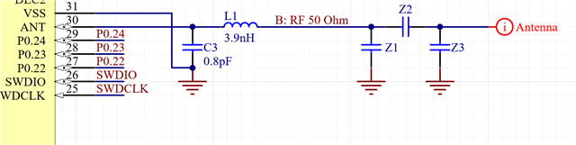
Fig.1
QFN - nRF52840/33/20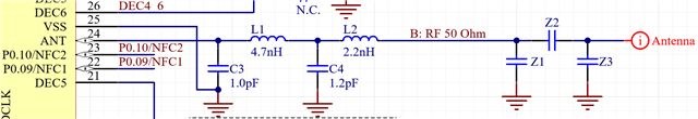
Fig. 2
WLCSP - nRF52833/40/20/11/10/05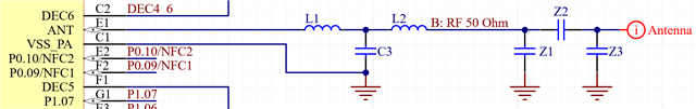
Fig. 3
Figure 1, 2 and 3 show the ANT pinout of the nRF52, the radio matching network, the 50 ohms reference point B, a matching network for the antenna and an antenna.
The matching network circuitry topology for the radio will vary from chip to chip, but the effect of the matching network is the same. Note for the QFN packages, the shunt capacitor closest to the radio should be grounded via the VSS pin closes to the ANT pin. This is to achieve optimal RF performance and is a part of the filtering effect to suppress the harmonics. See figure 4. 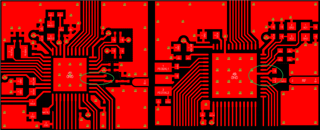
Fig. 4
This also means that the layout of the RF path should be directly copied from the reference design, as this plays a role in suppressing the harmonics and is necessary to pass the various regulatory standards.
It is difficult to copy the reference layout one to one directly, since differences in substrate, the number of layers, the length of transmission lines etc. can differ. This is why tuning the values of the components is needed to achieve optimal RF performance for each custom design.
How to tune the radio matching components?
Now we know that the matching components should match the output impedance of the ANT pin to 50 ohms, but also works as a filter to suppress the 2nd and 3rd harmonics. This means that when tuning the component values, both the fundamental output power and the harmonics levels must be measured.
The component's values are adjusted until the desired level of the fundamental outpower and harmonics are achieved.
Tuning the matching network is something Nordic can do for you, just create a private DevZone ticket, and ask for radio tuning.
For more information, you can also read the white paper RF performance test guidelines.
Typical mistakes you should try to avoid
Routing directly under the RF path
There cannot be any routing directly under the RF path. You want a solid ground plane under the RF path, working as an RF shield and reference ground for the transmission line. This solid ground should be covering the hole center pad of the nRF52, and go all the way to the antenna feed. On PCBs with more than two layers; add a keep-out area on the inner layers directly below the RF path (from ANT, pin on the nRF, to the antenna feed) to reduce stray capacitance.
Not having a 50 ohms coplanar waveguide
It is very important to include ground around the RF path to isolate it and make it more resistant to noise. The 50 ohms transmission line should be a coplanar waveguide. Use a calculation tool to calculate the width, W, of the track and the distance to ground, G, to get a 50 ohms transmission line. This is also essential to be able to perform conducted measurements. See example using AppCAD in figure 5.
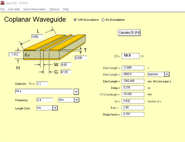
Fig. 5
Antenna – 2.4 GHz
Antenna choice is complex and depends on many factors, so spend some time finding an antenna that meets the needs of your specific design.
In Nordics example designs, you can find a monopole and a meander antenna, both printed PCB antennas, that you can copy and add some extra length for tuning.
Monopole quarter wave, printed PCB antenna: This antenna is easy to make and easy to tune, and it only needs one shunt components for impedance matching in addition to the antenna length. Space: About 23 mm long and needs a minimum of 5 mm clearance to the ground plane.
See the white paper on monopole quarter wave antenna.
Meander, printed PCB antenna: This antenna type requires a smaller area than the monopole antenna, but it needs a pi-network for impedance matching in addition to the antenna length.
See the design files for Nordic’s nRF52840 dongle, to see the meander antenna.
Other printed PCB antennas: There are multiple other options for printed PCB antennas; you can design your own or find them online. If you copy/reuse a printed PCB antenna, make sure you also copy the distance to the ground plane and add a suitable matching network for the antenna.
Off-the-shelf chip antennas: There are numerous chip antennas to choose from, and the antenna vendors can also help with the decision-making of choosing the right antenna for your design or provide an easy antenna selection guide. Pay attention to the recommended mounting for the antenna when choosing an antenna and make sure to follow the reference design, and ask the antenna vendor for review in addition to the review from Nordic on DevZone.
Power supply
To prevent noise from one source from affecting the others on the same PCB, we recommend using start routing. This means each supplied device will have its own track from the power supply. The center of the star network should be placed close to the power supply.
Normal or high voltage mode: VDD pins must be connected externally for both alternatives.
In addition to using star routing, a good ground plane is essential for reducing the risk of power noise.
Ground planes
The reference design from Nordic typically consists of two (a top and bottom layer) or four ground planes (a top layer, inner layer one, inner layer two, and a bottom layer). All ground planes should preferably be as large and solid as possible, and having four ground planes compared to two gives more freedom for routing and component placement.
Ground is the system's reference, as it is for the 50 ohms transmission line, and it is also the return path for noise. The larger the ground planes are, the more difficult it is to disturb them.
The ground planes should be connected by using via holes. Pay attention to the number of vias in the center pad of the nRF52, this should be copied from the reference design.
In general, add a via to ground near every ground pad of a component, add vias on the side of the RF path, and for larger ground areas; add a via at least every 5 mm. Try to avoid small ground islands (local ground areas). When they occur, add multiple vias to ground to ensure proper ground of the components connected to this ground.
Decupling capacitors
In Nordic’s reference designs, there are decoupling capacitors on the VDD (power supply) and DEC pins. These must be placed close with short tracks to their respective VDD/DEC pin.
The crystal oscillators
On nRF52 an external 32 MHz crystal is mandatory, and an external 32 kHz crystal is optional. When choosing a crystal it is important that it is within the specifications given in the product specification.
Load capacitors
The load capacitors, Ccap, are connected to the crystal and the values of the Ccap are given by the formula:
Ccap = 2*CL – C_pcb – C_pin
CL is the load capacitance of the crystal in use and can be found in the datasheet of the crystal.
C_pcb + C_pin is approximately 4 pF for the HFXO pins and approximately 5 pF for the LFXO pins.
More details can be found in the whitepaper "Crystal Oscillator Design Considerations". Please note that this paper is written for older chips (not nRF51/52) and that the input capacitance is given by: C_pcb + C_pin and not 1 pF, as it's stated in the whitepaper.
Frequency accuracy
For the 32 MHz crystal, the values for the load capacitors should be adjusted/altered if the frequency accuracy is not satisfactory, it must be below 40 ppm.
Measuring the frequency accuracy should be done by measuring the carrier frequency of an unmodulated carrier transmitted by the radio. If the carrier is measured above the center frequency, then increase the values of the load capacitors. If the carrier is measured below the center frequency, then decrease the values of the load capacitors.
This adjustment of the load capacitors is something Nordic can do for you during the radio/antenna tuning process.
Component placement
When designing a PCB with a radio onboard, consider the entire PCB as an RF PCB. Noise on the board can result in noise on the radio, causing problems during regulatory certifications.
When starting to design an RF PCB, begin by placing the antenna and antenna clearance area. The antenna should be placed as open as possible, giving it space to resonate.
When the antenna is placed, you can move on to the rest of the RF part of the design, RF path, matching networks, and the nRF52. Make sure to have room for all the required components in the reference design provided by Nordic.
Place the rest of the components.
Routing tracks: Use one layer for tracks first and move on to the other layers when needed. One layer should preferably be mostly solid ground.
Top Comments