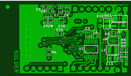
This post is older than 2 years and might not be relevant anymore
More Info: Consider searching for newer posts

Nrf51822 custom PCB BLE not detecting,but rest of the GPIO is working

GerberVINR-178.zip

SchematicVINR-178.pdf

Bottom layer

image description

Top Layer

image description

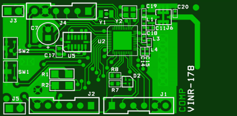
IC on the PCB is marked as follows: nrf51822 QFAAHO 1627WM. I am able to program the custom board from nrf51dk through SWD programming.I have enclosed the custom board's schematic for your reference.

I connected an led to P0.9 and did a blink test and it works fine.So I am assuming that GPIO pins and programming of my custom board is ok.When I upload the ble uart example on my custom board.The nrf uart app(android phone) is unable to detect the board.This example works fine with the beacon board and the nrf51dk.I am using nrf51 sdk 12.3.0 and soft device S130

  • Could please you post a picture of your layout surrounding the chip and antenna in addition to the schematic?

  • Do you have a ground plane on the bottom layer underneath the components leading out to the antenna?

  • Thanks for the response.Please let me know if this is what you needed to see apart from the schematic.I got this design from a freelancer online.I don't know whether we have a ground plane on the bottom layer underneath the components leading out to the antenna.I have posted the image of the top and bottom layer of the PCB.

  • Hello Vasanth

    In the layout I can see there is a bit of ground plane missing underneath the chip itself, C18 and C19. This is not optimal as the ground-plane underneath components conducting high frequency signals is very important, and it should be as whole as possible. Holes in the ground-plane will affect the circuit's impedance, causing a mismatch with the antenna. At a glance the antenna itself seems a bit short, which would affect antenna impedance and radiation characteristics.

    The components in your matching network (L3, L4 & C18) are not correct. You state you are using the nRF51822 QFAA. However, the components in your schematic corresponds to the QFAC packet. Please see the QFAA reference schematic, section 11.3, page 82 of the nRF51822 product specification. I also recommend you read through the PCB guidelines stated in section 11.1, page 79 of the PS, as well as this blog.

    I would recommend you try to change the matching components to the correct values, as this will bring the impedance close to 50 Ohms and see if you get a connection. The capacitor C20 in your schematic will need to be tuned along with the antenna length to provide a 50 Ohm match, see the above mentioned blog. I would also recommend you correct the layout, and use the layout of the nRF51 development kit as reference. You can find the hardware files for the devkit here, they can be viewed with the free version of Altium designer (Altium viewer).

    Best regards

    Jørn Frøysa

Related