This post is older than 2 years and might not be relevant anymore
More Info: Consider searching for newer posts

nrf51822 Custom PCB Questions

Hey,

I am currently designing a custom PCB w/ the nrf51822 QFAA. This is the first PCB I've designed and I'd really appreciate any help.

1.) Since I am using BLE I am not using the internal buck converter. I am planning on using a 3V battery and directly powering my nrf51 and two sensors with it. My sensors require 3V although I've read it would be most efficient to power the nrf51 w/ ~1.8V. Would an external voltage regulator be worth adding for my case?

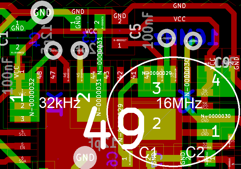
2.) I am mounting a coin cell battery on the other side of the PCB to save space. One of the VCC pads is under the 16 MHz clock. Do you think this will cause any problems?

3.) To save space I am not using the J-link debugger 10 pin header on my board. Instead I am planning to add vias and solder wires to program the nrf51822. Do you think this is OK? Will I need to add any external resistors to SWDIO or SWCLK?

4.) Lastly would it be wise to connect any GPIO pins I'm not using to ground or should I leave them NC?

Thanks!

  • Q1: The external converter could save you some power consumption, but it will cost more. So it's a trade off you have to do. It's usually an addition done in application where battery life time is a major factor and where the battery capacity is small. There's no straight forward answer as it will be up to what parameter is important to you.

    Q2: I would avoid having a VCC/VDD directly under the crystal if there's no shield in between. Are you able to rotate either the crystal or the battery holder in such a way that they are not directly over/under each other? The concerns is that you could have coupling of the 16 MHz onto the power supply of the chip and this could in return be modulated by the radio onto the carrier. Worst case is that you application have shorter range. It all depends on the amount of "noise" from the 16 MHz that reaches the power supply.

    Q3: This is fine. You need four pins, VDD, GND, SWDIO and SWDCLK. SWDIO and SWDCLK have internal pull on the chip, so you don't need external.

    Q4: You can do either, but leaving them NC is probably the most common thing to do and then controlling them from your code to make sure they are not floating.

  • Hi,

    to avoid duplication I will add my PCB question here. Is it ok to put external 16MHz crystal (with capacitors) on the bottom layer of PCB whilst chip is located on top layer? Where vias size are 0.7mm / 0.4mm.

    pcb fragment image: nrf_crystal.png

  • For Q2: Does this issue apply if the LF crystal and HF crystals are placed under the Battery (coin cell) Ground pad (opposite layer)?

  • In general for the HF Clk it is best to not the signal thru Vias. Since 16MHz could potentially cause some radiation at the vias. Better option would be to put the 32.768kHz on the opposite side and keep the HF crystal as close as possible to the chip.

Related