This post is older than 2 years and might not be relevant anymore
More Info: Consider searching for newer posts

nRF51822 - Poor RF performance on custom PCB

Up to this, we've been prototyping with MDBT40 module in our prototypes. We want to move to a completely custom PCB using the nRF51822 SoC for a number of reasons (space and design flexibility being of most concern).

I've already designed and populated the first PCB, and it has really poor RF performance. Data flows fine if I keep the device a few cm from my laptop antenna, but as soon as I move away it starts dropping. I was wondering if anyone could take a look and help me revise it for the next iteration?

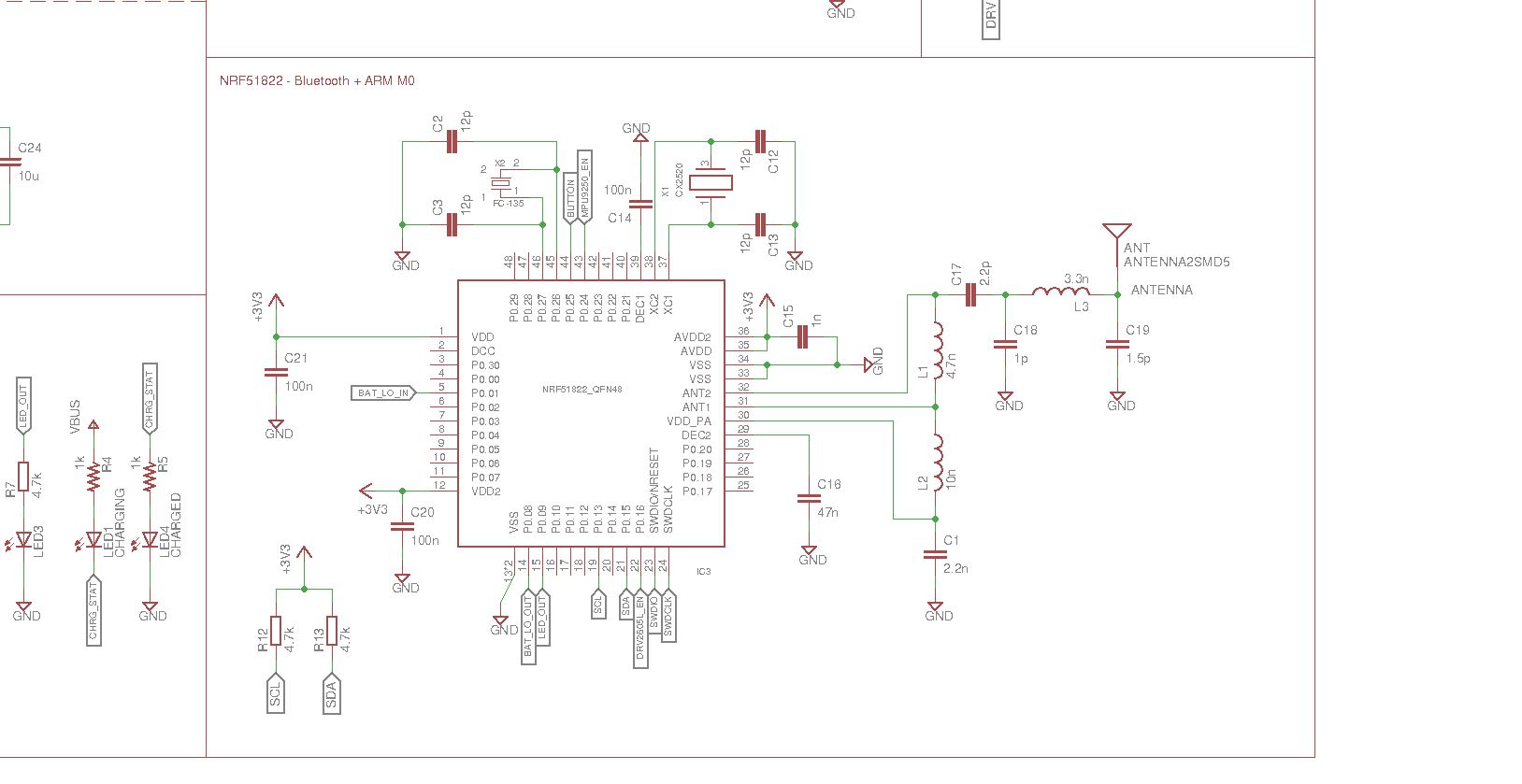
We're using the QFAA variant. The schematic was drawn with reference to the product specification (see page 79). The relevant part of the schematic can be seen below (full resolution).

schematic

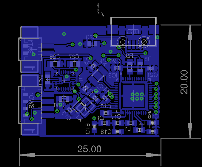
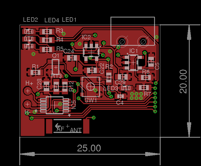
I've included snapshots of the top and bottom layers of the PCB. See below.

pcb bottom

pcb top

This is the antenna used for this design: www.mouser.com/.../ANT-xxx-CHP-x_Data_Guide-11938.pdf

Some notes I've gathered on this problem:

  • Poor grounding. The RF network ground has a long way to the SoC ground. There is a keepout below the RF network components. From the product specification, I can see that there is a ground plane below the components, so it should be ok to remove that keepout.
  • Antenna spacing. There are traces and ground planes close to the antenna, but no ground plane or traces below it. Is this a problem?
  • Tuning. The layout is almost copy-pasted from the product specification. Do I need any external components to tune the antenna?
  • Baluns. Would you recommend a single balun chip over seperate components?

And one more thing: From the product specification, looking at sections 11.3, 11.4 and 11.5, the component values for the RF network vary slightly between the 16kB and 32kB RAM variants (QFAA, QFAB and QFAC). Is there a specific reason for this?

Product specification: infocenter.nordicsemi.com/.../nRF51822_PS_v3.1.pdf

  • Does that antenna trace really go through a via to the other side of the PCB or am I reading this incorrectly? For a start you need a 50 ohm, or as close as you can get it, line from the SoC to the antenna, look up 'microstrip impedence calculator' online. And I know of no way to put such a line through a via and maintain the 50 ohm-ness.

  • Hi, thanks for the response. The line does indeed go through a via to the other side. The reason was that the pcb goes in an enclosure with a battery, and the antenna facing inward towards the battery was something I thought might mess up the transmission. Looks like that may have had the opposite effect :)

    I might try to move the antenna and cut the connection to the via and see how that goes.

  • hopefully you'll get some other replies from the nordic guys, which is why I didn't write an 'answer'. That was just the first thing I saw.

  • There are several important problems in the layout, and you have noted the most important things yourself:

    • The grounding must be improved significantly. You should have a larger and more solid ground plane. As you have such a cramped PCB the ground plane is separated by a lot of long traces, which result in high series inductance, and thus high RF impedance and bad grounding. In this case I would recommend adding a 3rd layer with a ground plane. You should connect the ground planes of the top and bottom to the middle ground layer with a lot of vias. Remember to cut a "hole" in the inner ground layer under the matching network. I recommend you to first place the antenna, then place the radio and matching network close to the antenna, exactly copying the reference layout.

    • The antenna should be placed as freely as possible and in accordance with its datasheet. The antenna feed should be a proper 50Ω microstrip line. (For example the free AppCAD tool can be used to calculate the transmission line)

    Your other two points are less important, but also worth consideration:

    • In practice, you will usually need to tune the antenna (even though the datasheet states that it is not needed), as non-optimal placement can de-tune the antenna, so that it is no longer 50Ω.

    • Since you are restricted on space, a single chip balun may be a good choice.

    Regarding the differences in component values in the RF matching network for the 16kB and 32kB variants in the reference designs, this is due to different die sizes, and hence different lengths of the bonding wires.

    You might want to check out the following links:

  • Thanks for the reply! I've re-designed the board and created another thread here. Could you look it over and see if there is anything obvious that stands out?

Related