5V vs 3.3V

We're trying to reduce noise inside a device using the NRF9160 and the last noisy device we have is a 6V -> 3.3V switching power supply for the nrf.

One idea on the table now is to replace the switching supply with a linear one, but dropping from 6V to 3.3V using a linear reg would increase battery consumption too much. However, powering the nrf from 5V would make it feasible - at least in theory. 

All our peripherals are either 5V tolerant or already 5V and using level converters from 3v3 to 5V, so this is not an issue.

In terms of usage, it's an IoT device sleeping a lot, with regular (every 200ms up to 1s) wakeups to read some sensors quickly. There is modem activity once in a while, as the cell tower demands.

So the question is - is there any major difference in power consumption when running the nrf9160 from 5V vs 3.3V? I see that the sim is using 1.8V but that one is already generated internally I presume. Is there anything else we should be aware of when powering from 5V?

Thanks a lot for the support!

Parents
  • Hello,

    The nRF9160 has a single main power supply VDD. The internal components are powered by integrated voltage regulators. Th GPIO input/output supply is independent of VDD through VDD_GPIO. This enables easy match to signal voltage levels in the PCB.

    You can see from the table 3GPP compliancy is 3.3V (Including voltage drop, ripple and spikes.RF 3GPP compliancy requires 3.3 V)

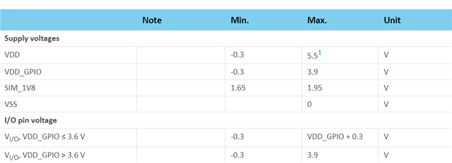
    The supply voltage VDD of nRf9160 is ranged as -0.3 to 5.5V and VDD_GPIO is -0.3 to 3.9 V. But these 5.5V and 3.9V are the absolute maximum ratings. Maximum ratings are the extreme limits to which the chip can be exposed for a limited amount of time without permanently damaging it. Exposure to absolute maximum ratings for prolonged periods of time may affect the reliability of the device.  

    It is not recommended to use high voltage with high frequency, high capacitance loads unless needed, as this may increase noise level and affect radio receiver performance. High drive/high load should especially be avoided on GPIO pins close to the radio front end.

    I think if the source is 5V, you should use a DC-DC converter to keep the voltage down in an efficient operative range. 

    Thanks.

    BR

    Kazi

Reply
  • Hello,

    The nRF9160 has a single main power supply VDD. The internal components are powered by integrated voltage regulators. Th GPIO input/output supply is independent of VDD through VDD_GPIO. This enables easy match to signal voltage levels in the PCB.

    You can see from the table 3GPP compliancy is 3.3V (Including voltage drop, ripple and spikes.RF 3GPP compliancy requires 3.3 V)

    The supply voltage VDD of nRf9160 is ranged as -0.3 to 5.5V and VDD_GPIO is -0.3 to 3.9 V. But these 5.5V and 3.9V are the absolute maximum ratings. Maximum ratings are the extreme limits to which the chip can be exposed for a limited amount of time without permanently damaging it. Exposure to absolute maximum ratings for prolonged periods of time may affect the reliability of the device.  

    It is not recommended to use high voltage with high frequency, high capacitance loads unless needed, as this may increase noise level and affect radio receiver performance. High drive/high load should especially be avoided on GPIO pins close to the radio front end.

    I think if the source is 5V, you should use a DC-DC converter to keep the voltage down in an efficient operative range. 

    Thanks.

    BR

    Kazi

Children
Related