This post is older than 2 years and might not be relevant anymore
More Info: Consider searching for newer posts

50 Ohm track for 4 PCB Layer (NRF51822-QFAC)

Hi,

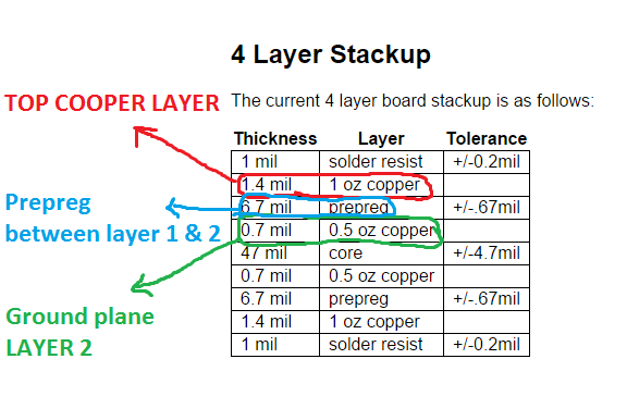
I designed before my board for 2 layer PCB and i used the coplanar waveguide with ground-plane in the bottom. now i want to move to the 4 PCB layer and i choose the ground-plane as the layer number 2 just above the top-layer, and i have some doubt about the design.

as known the track width depend on the characteristic of the board in order to match 50 Ohm, like the cooper thickness, the distance between the top layer and the Ground-plane layer....

i will make the board with oshpark and here the Fabrication Spec here : docs.oshpark.com/.../

above a screenshot of the calculation that i made to determine the track width :

image description

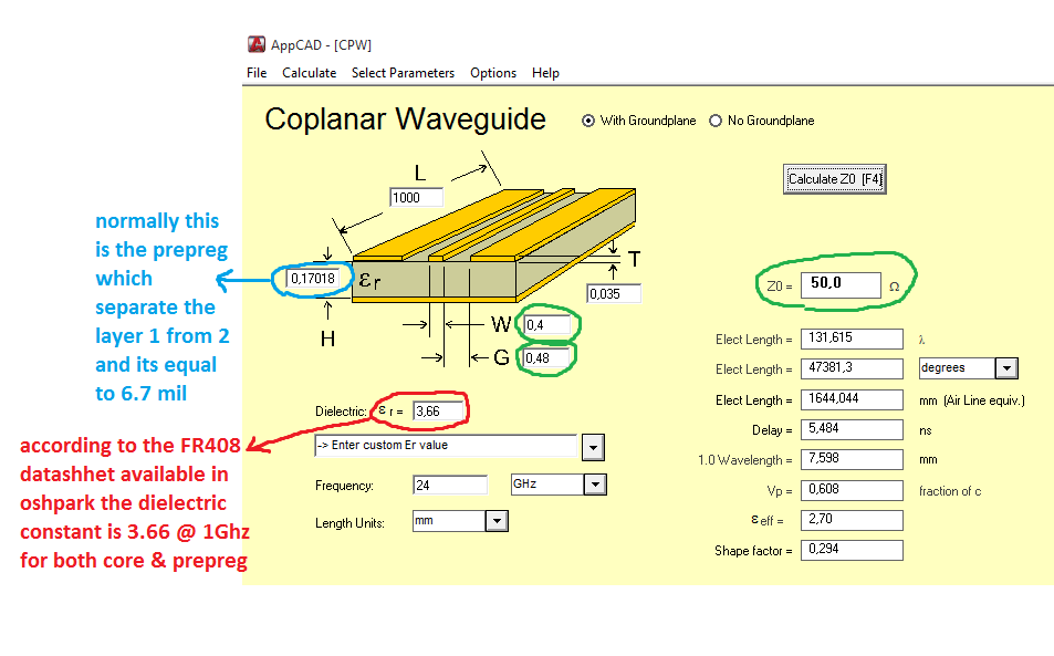
as described in the oshpark 4 layer spec the separation between the top layer and the layer number 2 is the prepreg which width is equal to 6.7mil = 0.17018 .

image description

and the dielectric is equal 3.66 @ 1Ghz according to this docs.oshpark.com/.../FR408-High-Performance-Laminate-and-Prepreg-Data-Sheet.pdf

Here's how it look like my board :

image description

i choose the PI network components with 0402 dimension to be as closest as possible to the track width.

are my calculation correct ? did i made something wrong ?

Regards,

Parents
  • Hi,

    The calculations looks correct. Since you have a "keep out" area in layer 2 and 3, just below the transmission line, you can treat the PCB as a 2-layer PCB for the calculation.

    The PI-network also looks good. One thing I have to comment on (since it's not included in the image of the layout) is that you should place a GND VIA close to the BALUN to ensure it's grounded properly. You might have already done this, but I'll comment on it just-in-case.

    All in all; Great work, Tizana!

    Cheers, Håkon

Reply
  • Hi,

    The calculations looks correct. Since you have a "keep out" area in layer 2 and 3, just below the transmission line, you can treat the PCB as a 2-layer PCB for the calculation.

    The PI-network also looks good. One thing I have to comment on (since it's not included in the image of the layout) is that you should place a GND VIA close to the BALUN to ensure it's grounded properly. You might have already done this, but I'll comment on it just-in-case.

    All in all; Great work, Tizana!

    Cheers, Håkon

Children
No Data
Related