VDD disconnected and VBUS connected

Hello,

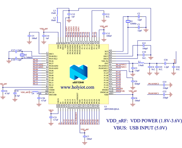
I have designed a keyboard around the nRF52840. The VDD is being used, not the VDDH. If the keyboard is attached to USB, VBUS is fed into a battery management IC and charges a LiPo battery, also goes into a LDO and the stabilized 3.3V VDD is fed to the nRF. If the keyboard is not connected to USB, it is powered through the battery management IC -> LDO -> VDD.

In order to shut off the keyboard and prevent draining the battery, I have a switch cutting the power path between the LDO and the VDD net.

My question: Is it OK to have the switch off and still have the device connected to USB, feeding power into the VBUS pin although there is no power going to the VDD pin? I am not concerned about eventual power consumption of the nRF52840 chip itself, only if this a supported or unsupported configuration.

Thanks for any responses and if I shall rather open a new thread with this question.

  Michael.

PS: this is the schematic for one of the halves of the keyboard.

nightliner.pdf

Parents
  • You're fine in using only VUSB whilst VDD is disconnected from Battery IC/ LDO. I do assume that you've used one of the reference designs of using VUSB.

    Regards

    Shahid

  • Well, the module is from holyiot and it seems to be very closely modelled after reference configuration no.5 from your data sheet. 

    The main difference that I found is, that in your reference design VDDH is tied to VDD and in holyiot's module it is tied to GND via a 4.7uF cap.

    I merely added two 10uF decopling caps close to the LDO and to the holyiot module for VDD and added ESD protection, reverse feed protection to the VUSB line.

    I hope that makes sense, I am now going to populate the board... Wish me luck :-)

  • If you are not using VDDH as the power source you HAVE to connect it to VDD as leaving it unconnected is a violation of the specification of the part.

    In the module it is probably left unconnected to allow you to power the device through it, not limiting the functionality, with the intention that you will connect it on the outside if not used.

  • That is a problem then, because the VDDH pin is not exposed to the outside of the module. I posted the design document of the module in my second post above. It is not "unconnected", it is connected to GND via a capacitor. I wonder, why a company would deliberately choose such a design - maybe in an earlier Nordic design document, it was recommended differently? Since I do not have any other options, I have to use the module as-is and if it blows up, then I have to choose a completely different vendor and redesign the PCB. To design a PCB completely on the PCB without a module would mean I would have to design the Bluetooth antenna as well and that is a territory, where I have no idea how to tackle that, as it involves to design the PCB traces according to the materials used and factory process of JLCPCB in order to get impedance matching and such stuff. And I have only KiCAD, not some fancy Altium Designer or so... If you have any pointers, how to go about this, I would certainly love to try that!!! The more I can learn, the better!!!

  • As per my experience, you can also leave VDDH floating/ unconnected it won't create an issue. But, I cannot suggest connecting to the ground using a cap as I have not used such a configuration.

  • It will usually work but if you run into problems you may be on your own as the design does not comply with the device specification. For testing shouldn't be an issue but for production I would say no.

  • Thank you very much both of you for your suggestions and help!

    It seems I should start learning more about antenna design with KiCAD. Need to find some pointers on the web that could help me in this new endeavour. I'll let you know, if the board works ok or what kind of issues I will encounter.

    Thanks again and have a wonderful 2024, everyone!

Reply Children
No Data
Related