Noise on PCB during 2.4GHz RF transmission

Hello friends, 

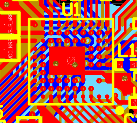
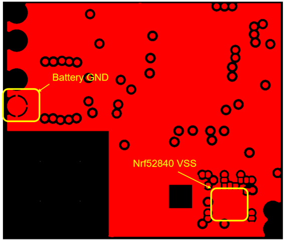
I am using nrf52840-CKAA for my customize PCB. 

I am facing the noise during RF transmission on my ADC. The peak noise happen when I send a packet of data via RF antenna. 

Power_Tx = 4dBm


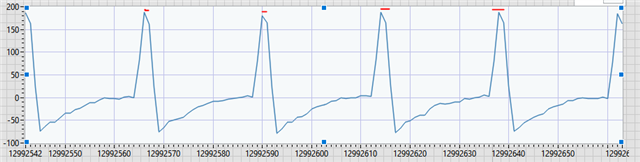
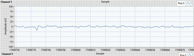
When I decrease the Tx Power to -12dBm, the peak noise was gone.

I wonder that MCU takes a lot of power during RF transmission so it affect to the stability of power line. 

In nrf52840-CKAA, currently I tie all VSS pin together instead of tie each of them directly to the GND plane. Is it the problem? 

I appreciate all your suggestions. 

Minhduc

  • Hi

    What pin(s) are you using for ADC on your nRF52840 SoC? As you can see in the nRF52840 pin assignments section, some GPIOs are recommended to use at standard drives/low frequencies. That is because these are located near the radio, and can affect radio performance. It is also thus possible that the radio can affect pins/lines that goes close to the ANT pin/trace. 

    Regarding your second point, I will need to check that with one of my more "HW oriented" colleagues and get back to you. Thanks for your patience!

    Best regards,

    Simon

  • Glad to hear from you Simonr. When I mentioned "ADC", it was the external ADC instead of nrf52840-ADC.

    I locate that external ADC quite far from the ANT trace (around 2cm).

    Best regards,

  • Hi

    Can you share your HW files so we can do a review of schematics and the PCB you're using? Here is an image of how the ground plane and VSS pins should be connected. 

    Also, please share some more details on the ADC you're using. What are you measuring on it, and what is this external ADC exactly? And is it connected to the nRF52840 somehow? If so, to what pins on the nRF52840.

    Best regards,

    Simon

  • Hi Simonr, 

    My ADC is Intan chip RHS2116. It is controlled by MCU via SPI communication. 

    Instead of connecting all VSS at top layer ground plan, I use uVia for each VSS pin for connecting it directly to the layer 2 ground plane. 

    In my PCB, I use a lot of via so it limit the return path. Do you think it is a possible reason? 

    Best regards,

  • Hi

    I will have to wait for some of the HW engineers to come back from Easter vacation, so someone will be able to help you Tuesday April 2nd. In the meantime, can you upload the full schematics and gerber files of your design so we can conduct a proper HW review on our end? If you'd like I can set this case to private mode so the files you upload will only be visible to yourself and Nordic engineers.

    Best regards,

    Simon

Related