Hi
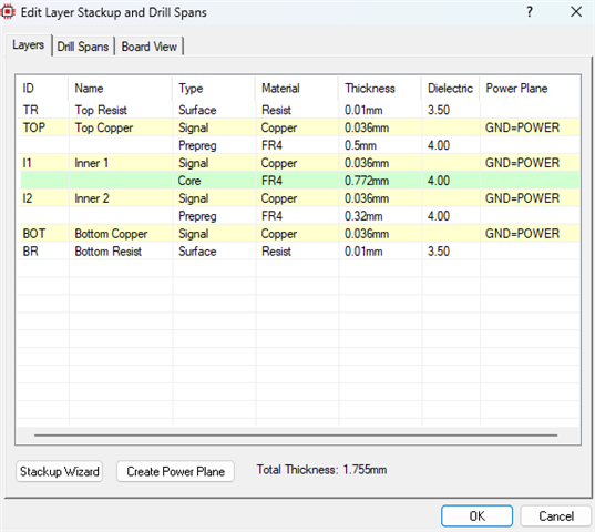
I am designing a 4-layer pcb. How much do you think my signal trace thickness should be?
I use https://www.trgcomponents.de/en/ant-24-cw-rah-rps.html
connector —> www.ozdisan.com/.../954516
Hi
I am designing a 4-layer pcb. How much do you think my signal trace thickness should be?
I use https://www.trgcomponents.de/en/ant-24-cw-rah-rps.html
connector —> www.ozdisan.com/.../954516
I added nRF7002 IC. The distance between antenna and IC is 7.8mm. How many mm should I make the path thickness. I wanted to ask because I have little knowledge on this subject.
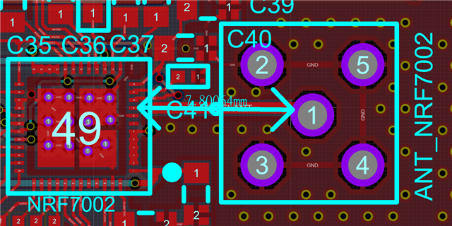
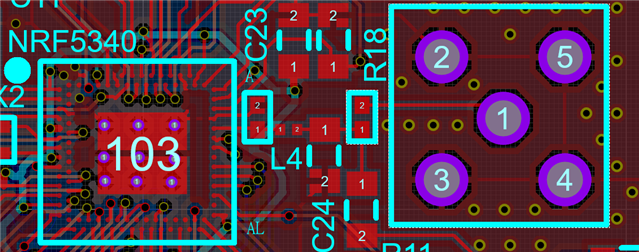
This is the NRF5340 Antenna layout.
Hi,
We have a guide on things here: (+) General PCB design guidelines for nRF53 series - nRF5x - Hardware design, test and measuring - Nordic DevZone (nordicsemi.com)
Thickness of the trace will depend on the PCB stack-up, you can use a tool calculate, some PCB design programs also have these features built in.
The nRF5340 needs a matching network on the ANT pin, this is the radio matching network ad does two things, filter harmonics and matches the output to ~50 Ohms 
Since you are using a connector you don't need the Z1,Z2,Z3 matching components as long as you RF trace is approximately 50 Ohms or if whatever you care connecting is not 50 Ohms either.
Regards,
Jonathan
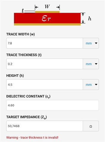
Is it correct to set it this way? If it is correct, will it cause problems if the thickness between PCB layers is more than 0.7 mm?
This looks fine, but trace width seems a bit big, are you sure that the values are correct? Trace width seems a little wide.
From the first image you shared in comment here it seems that the Hight is 0.5mm
Just using a online calculator here and i with the second layer as reference GND then thickness is less then1 mm for 50 ohms. 
Or here:
Trace Impedance Calculator | DigiKey 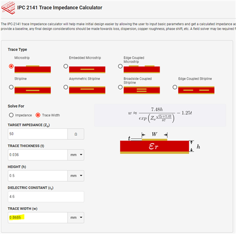
Muhammed said:will it cause problems if the thickness between PCB layers is more than 0.7 mm?
It will depend on how much different, if there is just minor variance then no big issue.
Regards,
Jonathan
This looks fine, but trace width seems a bit big, are you sure that the values are correct? Trace width seems a little wide.
From the first image you shared in comment here it seems that the Hight is 0.5mm
Just using a online calculator here and i with the second layer as reference GND then thickness is less then1 mm for 50 ohms. 
Or here:
Trace Impedance Calculator | DigiKey 
Muhammed said:will it cause problems if the thickness between PCB layers is more than 0.7 mm?
It will depend on how much different, if there is just minor variance then no big issue.
Regards,
Jonathan
Thank you for help.
Best regards,