Hello support.
A new design is looking at using nRF24L01+ to communicate wirelessly. I'm aware that this IC is no longer recommended for new designs, however, it's the one that is currently in the spotlight and being evaluated.
A custom PCB was designed to test the part and exceptional range was verified. To further the investigation, it was then integrated on another custom board with the microntroller used to control it. The layout was altered, but the designer paid more attention to recommdations for this release, so it should have been an improvement. However it was not. Range was greatly diminished. Yet another attempt was made trying to better replicate the example in the datasheet, and range was lacking again.
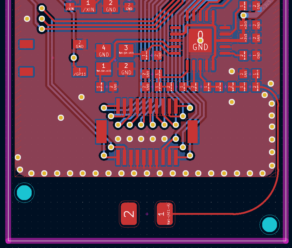
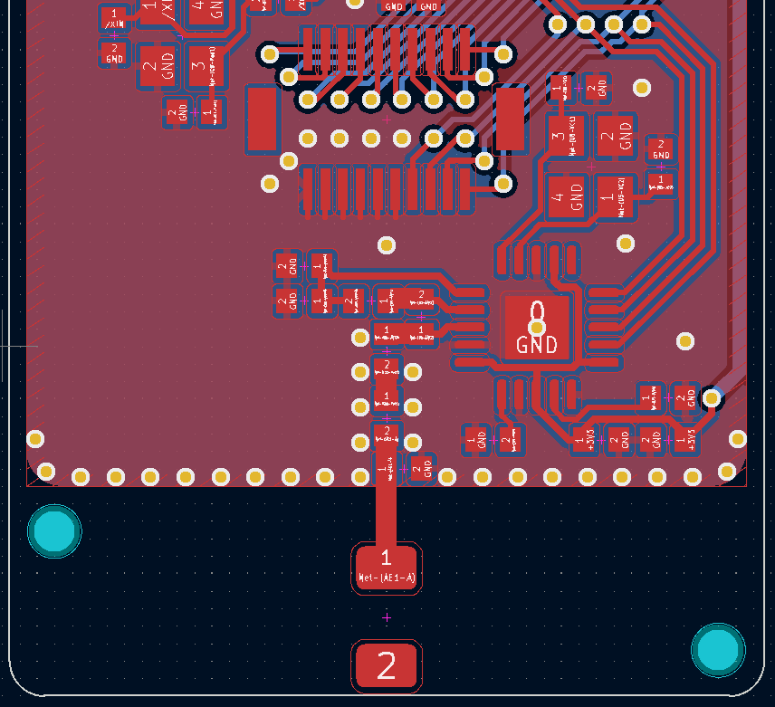
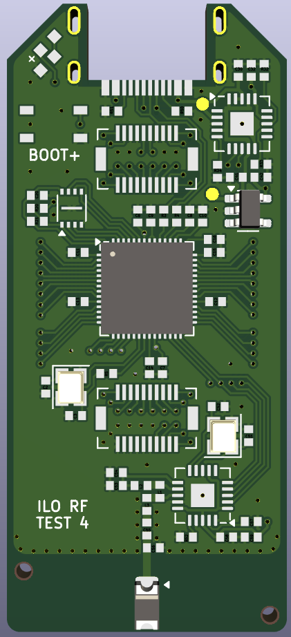
BOM wise, they were all built with same parts. It seems to be the layout that is the deciding factor. I'm wondering if you could look at the layout and see a smoking gun on why V2 and V3 don't work as expected, or why V1 does work properly. I don't have the layout of V1, but I have pictures:
V1 TOP
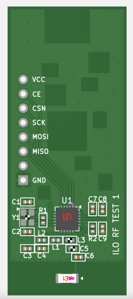
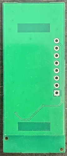
V1 BOT
V2 TOP/BOT
V2 3D
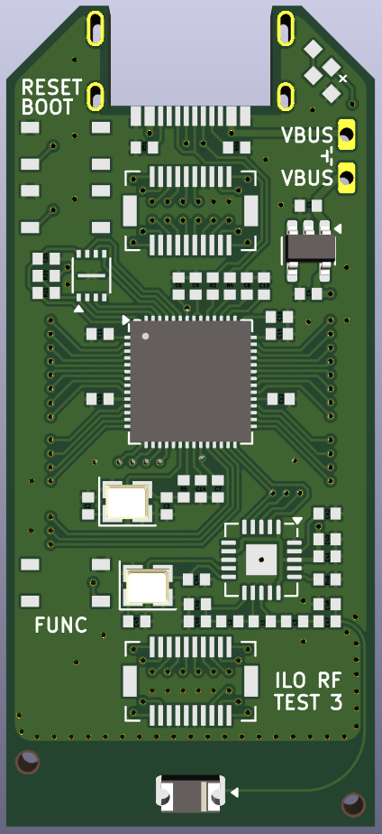
V3 TOP/BOT
V3 3D
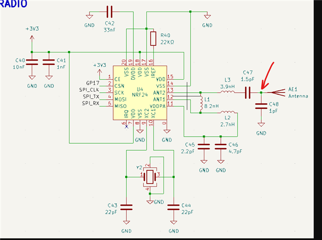
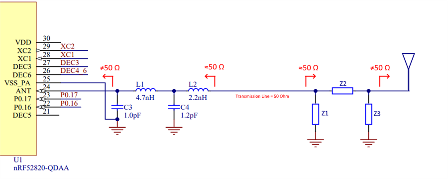
Here's schematic:
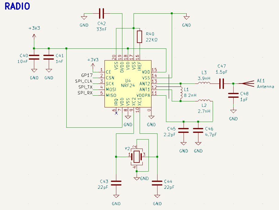
V1 does not have equal length ANT lines, which I know can be problematic, yet it works great. Maybe because of the cutout below the antenna tuning parts.
V2 has a long unmatched trace to the antenna, so I understand why that wouldn't work, but V3 takes care to place and route antenna tuning well. It has a nice solid gnd pour, unlike V2. What am I missing?
Any advice would be appreciated. Thanks!