nRF52832QFAA TX power readings

Hello,

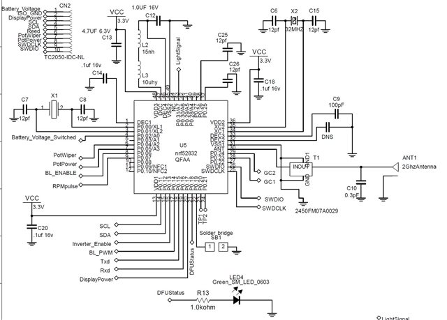
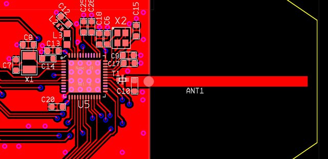
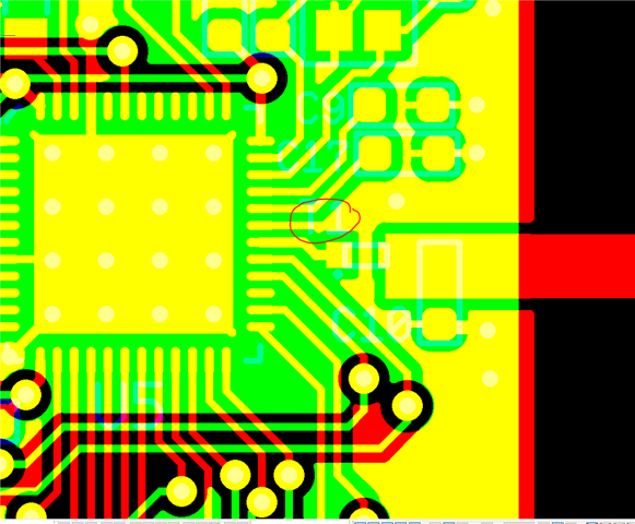
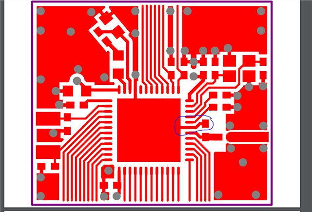
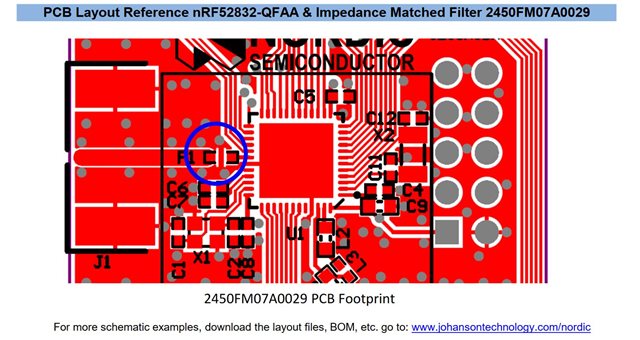
I have a nrf52832-QFAA design that came back from the emissions test lab and they told me that the TX power on the Radio Pin was around -6dBm at the low frequency (2402 MHz). The antenna was milled off and we attached a SMA connector to the output of a impedance matching LPF from Johannson (PN: 2450FM07A0029) to the single ended ANT pin on the nrf52.They are using the nrFConnect DTM program to set TX power to 0dB for testing, channel 37, LE 1Mbps, PRBS9 and 37bytes with no time out. This is my 2nd nrf52832 design and the first one passed at very close to 0dBm. I'm looking at them side by side to see what I did differently and was hoping for a few questions asked.

1) What will cause a drift in measured TX power to default set TX power? Will using the LDO or the internalDCDC affect this?

2) So far, the only difference I can remember would be the LPF layout, this design doesn't have two net 0/ground holes on the GND pins of the LPF. The first design I did has it. I don't think that's a big factor, I do have a third design that has that. Will test with that soon. Another thing about this design is I followed the nrf52 Internal DCDC recommended schematic and I had DEC3 with 100pf and left DEC2 a DNS. The first design that passed had both 0.1uF on the two pins, not sure if that will make a difference.

Here's layout and schematic.

Parents
  • Hi,

    1) What will cause a drift in measured TX power to default set TX power? Will using the LDO or the internalDCDC affect this?

    No, I don't think this is a result of DC/DC or LDO,do you see any difference whether LDO or DC/DC is enabled/disabled?

    The nRF52832 has a Radio accuracy of +-4 dB. However most devices will be within +-2 dB. 

    The schematic look ok, a bit more decoupling on VDD than recommended but I don't think that's related to what you observe. 

    Can you share the layout as Gerber files?

    regards

    Jared 

  • Hi,

    Here you go. I am suspecting it's the absence of the two ground vias at the LPF but I hope you can tell me better!

    Thanks

    Julius 

Reply Children
  • Hi,

    Pin 31 should not be connected directly to the GND plane, but grounded through the centerpad as in the reference design, this is very important for harmonic filtering, which can affect the measured TX power:

    regards

    Jared 

  • Hi Jared,

    The nrf52 reference design used an LC circuit on the ANT pin, I am aware of grounding the "ground" pin on C3 (from the reference design) to the nrf52 ground pad only with a keepout from the rest, I had that design in the very early stage of my first design.

    Now I am not using a LC circuit but a Johanson impedance matched LPF for the 50ohm transmission line on the ANT pin. See attached for their reference circuit implementing their LPF with the nrf52.

    I do see that I need to short pin 31 back to the center pad of the nrf52. Now to figure out how do I verify/test that theory..

    Thank you!

    Julius

  • Hi Julius,

    You're absolutely correct, I see now that the datasheet for the LPF specifies the pin to be connected to the GND layer. As for pin 31, it has to be connected to the centerpad, and unfortunately the only advice I could give you is to do a redesign. If you decide to do a redesign then I would also suggest using our matching network by placing the single components instead of using the LPF, as we have seen that placing the single components usually result in a better RF design in terms of loss. This makes it possible for us to optimize the matching network if you send it in for tuning. 

    regards

    Jared 

Related