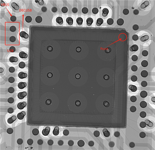
In my design, I choose to use the circuit suggested in Config no.5, but the USB interface is not effectively identified in the actual test. Through the test, the power supply of 5.0V can be measured on the VBUS pin (referred to as the USB interface), but there is no voltage measured on the DECUSB pin. Through the block diagram provided in the datasheet, I have eliminated the SMT quality problem by X-RAY, is there any problem that I did not consider during the debugging process or is there a problem with my schematic diagram?
PS:
1.At present, the board can burn the program normally, and the peripherals can also be controlled.
2.USB Demo selected the official course, the routine can run normally on the DK board .
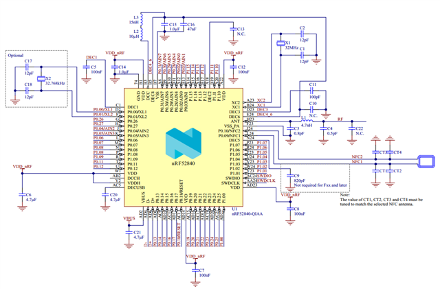
Nordic Config no.5 Circuit
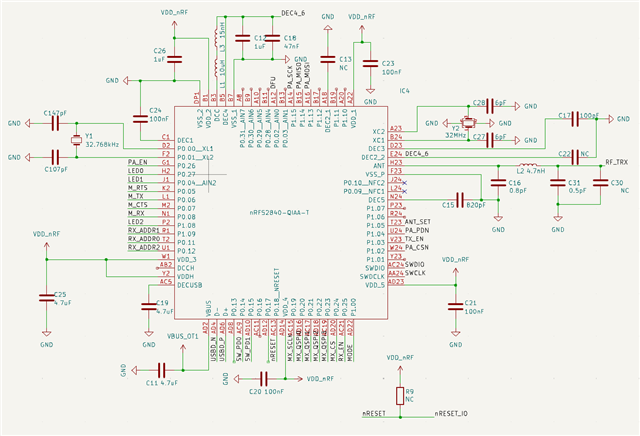
My design
Chip X-RAY