This post is older than 2 years and might not be relevant anymore
More Info: Consider searching for newer posts

Unable to connect with JTag

Hi, I'm working on custom PCB and I have small issue. After making PCB I was trying to connect, but no luck - "(unable to connect to the target)"

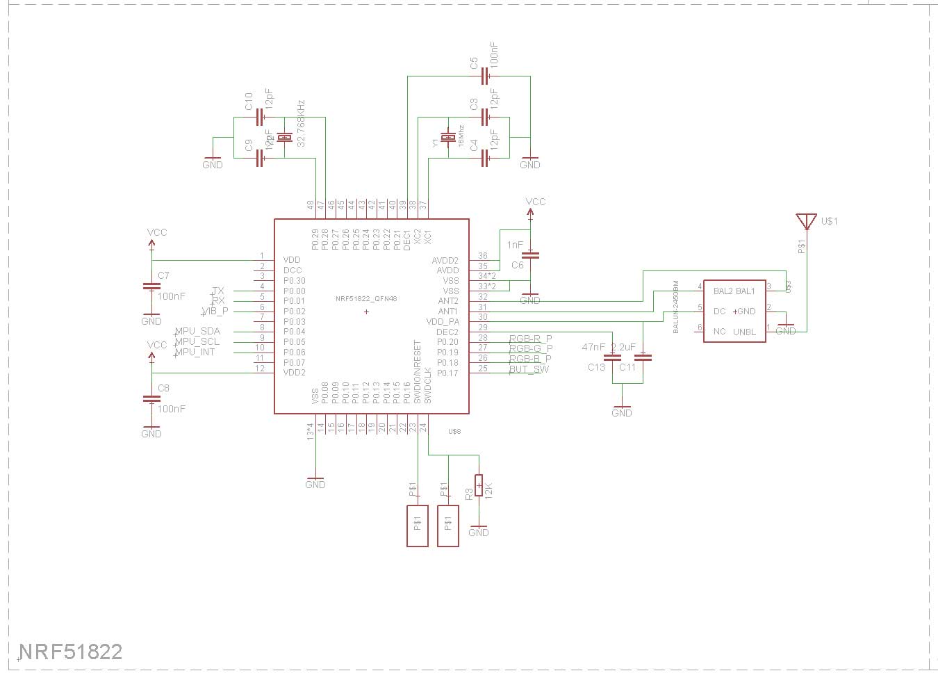
Maybe there is something wrong with my schema: image description
or maybe with PCB: image description

I have tested with different NRF chip, and also with different crystal.

What should I test ? How to verify that chip is working ?

Parents
  • Hi Robert,

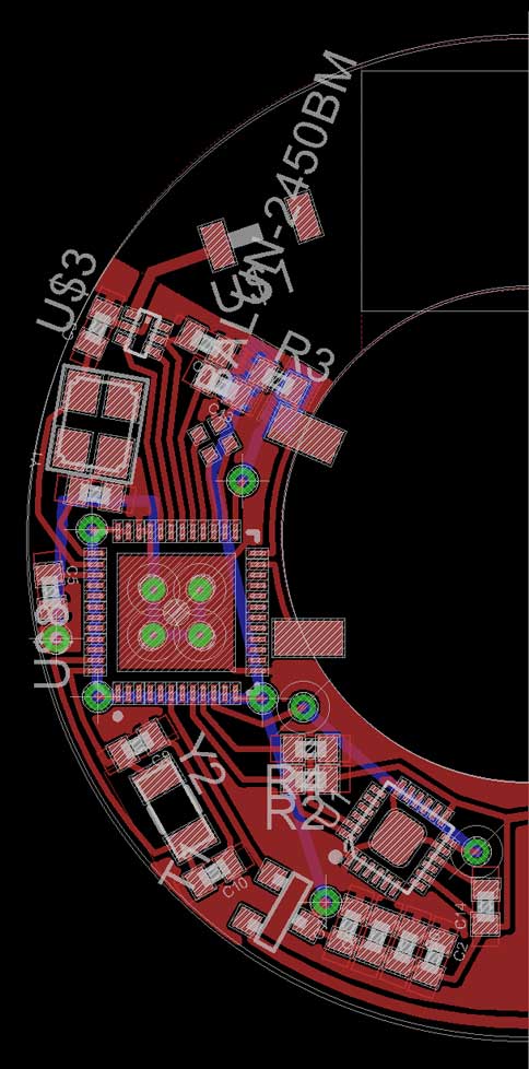
    There are several errors with your PCB. The RF part will likely not work at all. Please consult the general PCB design guidelines. And make sure that you follow the reference layout for your balun.

    The major error in your design is the long tracks from the nRF51 chip to the balun, these will shift the phase of each line, and the balun will not work as intended. The length of the lines are also not equal so the differential signal will be out of phase.

    Additionally it seems that you suffer from size constraints on your board, you might want to consider using the WLCSP package option instead, which has a much smaller footprint.

    We provide full reference circuitry with all necessary Altium files, these are available in CSP and QFN packet variants.

    If you are having trouble seeing how to connect programming pins or other, you can see how it is handled in the design files for the development kit or dongle.

    Hopefully this answers your questions. Best regards,

    Øyvind

  • Thank you for your answer Øyvind. I tihnk I know how to program through SWD.

    The problem that I discover is that after connecting power it does not consume current at all so something is wrong with PCB or chip that I used

Reply Children
No Data
Related