
hi
We have developed it to the specifications below and are preparing for mass production.
We would like to inquire about a 10% standby current test defect occurring in pre-production (100EA).
1. Specifications
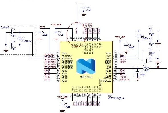
- nRF52832
- SDK 17.1.0
2. Self-review results
- PCBs with standby current defects continue to defect (100%)
- Normal PCB with no standby current defects continues to be normal (100%)
- If you retouch the nRF52832 IC with a heat gun, the standby current will return to normal for a while and then increase again.
- Changing peripheral devices such as crystal, LDO, etc. does not solve the problem.
- Normal current: 100uA -> defective PBA 230uA
=> Is there anything you can guess as the cause?

