Hello, Can use nrf52840-DK to program E73-2G4M08S1C module with nrf52840 or I need J-Link Edu Mini for that ?
Hello, Can use nrf52840-DK to program E73-2G4M08S1C module with nrf52840 or I need J-Link Edu Mini for that ?
Hi, Greg. I can't see a reason why you shouldn't be able to use the nRF52840 DK to do that.
The debug output section of the nRF52840 DK's PS describes how the custom board should be connected to the DK.
The description of the same subject in the nRF5340 DK's PS contains more figures, which may help understand what it should look like with the nRF52840 DK as well.
Best regards,
Mathias
Thank you Mathias,
Yes, I see outputs from DK:
| 3 | SWD1_VTG | Voltage supply from external target that is used as an enable signal for activating SWD1 |
| 4 | SWD1_SWDIO | Serial Wire Debug (SWD) data line |
| 5 | SWD1_SWDCLK | SWD clock line |
| 6 | SWD1_SWO | The Serial Wire Output (SWO) line is not used for programming and debugging over SWD |
| 7 | SWD1_RESET |
but what inputs on module E73-2G4M08S1C -
I found only:
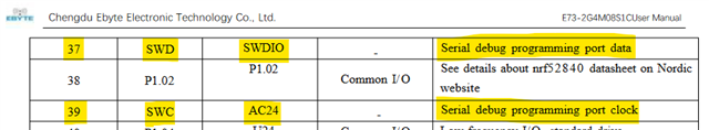
37 SWD SWDIO
39 SWC AC24 ???
Do you have a reference for connection - so I will not burn anything?
And which one I need - connectors P19 or P20 ?
So, you do not know how to connect!
Can you ask somebody how knows?
What have you tried to do so far?
Does your board have the standard 10-pin Serial Wire Debug (SWD) connector, so you're able to connect through P19? Or do you have to use a custom connection and connect through P20?
I am trying to order PCB for placing E73-2G4M08S1C module,
so I need a table with pin to pin connections to E73-2G4M08S1C inputs from nrf52840-DK outputs - P19 or P20 to program it:
mathiaso said:GS2 said:I found only:
37 SWD SWDIO
39 SWC AC24 ???That sounds right. From the module's datasheet:
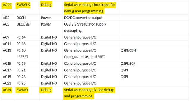
From the aQFN73 package's pin assignment list:
There you have the SWDCLK and SWDIO lines.
The following pins should be the ones for VDD, GND, and reset on your module. You'll find this in the module's datasheet, which I linked you to earlier.
Ensure that your device is powered during debugging and that the voltage on the external board matches that of the DK, as stated in the note here.
As you're creating your own board you're free to choose whether you use the 10-pin SWD connector found on P19 or if you want to connect through the P20 connector on the DK.
Thank you mathiaso,
Can you please verify and edit the TABLE I made based on above information:
| E73-2G4M08S1C | P19 | P20 | |||
| 19 | VDD | 1 | EXT_VTG Voltage supply | 3 | SH_VTG Voltage supply from |
| 21,24 | GND | 3,5 | GND Ground | ??? | GND Ground |
| 26 | RST | 10 | EXT_RESET | 7 | SH_RESET Reset line |
| 39 | SWC AC24 | 4 | EXT_SWDCLK SWD clock line | 5 | SH_SWDCLK SWD clock line |
| 37 | SWD SWDIO | 2 | EXT_SWDIO SWD data line | 4 | SH_SWDIO SWD data line |
What PIN will go for P20 GRD ?
Do I need:
P19.9 EXT_GND_DETECT Ground detect
P20.1 VDD_nRF nRF52840 SoC power domain
P20.2 VDD_nRF’ Main nRF52840 DK power domain
P20.8 SH_GND_DETECT Ground detect
Thanks.
Also:
1. Is his secure way for production programming?
2. What should I do to make the code locked - not readable?
Thanks again
Hello, mathiaso
No response - Are you OK ?
Hello,
Please make a new case for new questions.
Kenneth
You can close this ticket.