Custom PCB soldering issues

Hi, 

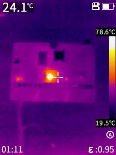
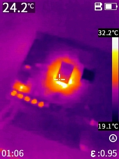
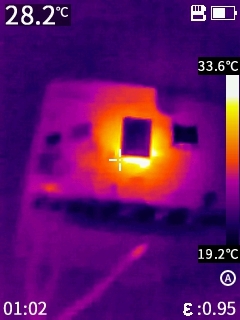
I am working on a custom PCB. I ordered them at JLCPCB and I have some issues with the soldering. I noticed in a few boards there is a short in the board between the NRF VDD line and GND. Using a thermal camera I found out there are multiple boards with multiple components getting hot when injecting power with limited current.
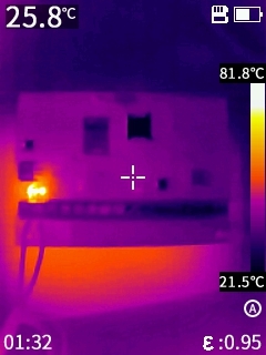
I set the power supply to 3,8V and current to max 80 mA. All shorts are gone when i removed the NRF9160 from the board by using a pre heater and hot air. 
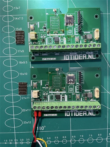
 I also added the Gerber file. Is there anything I can do to improve solderability to this design? 

nRF_Board_gerber.zip

Thanks!

Parents Reply Children
  • Thank you for sharing that document; it’s really helpful. I’ll reach out to JLC and request they bake the boards before assembly to see if that helps.

    To elaborate on the issues I’ve been experiencing:

    • Batch 1: I ordered 12 boards, but unfortunately, 4 of them were unusable.
    • Batch 2: Out of a batch of 20 boards, only one worked somewhat; the rest had issues, specifically short circuits within the NRF9160 footprint. This effectively makes the entire batch of 20 unusable.

    There was a difference in sourcing the parts. The parts from batch 1 where sources from Element 14 UK, the modules from batch 2 are from JLC directly. 

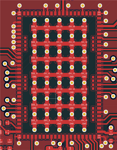
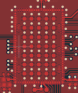
    Between batch 1 and batch 2 I did some changes in the ground layer to optimize it. 

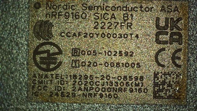
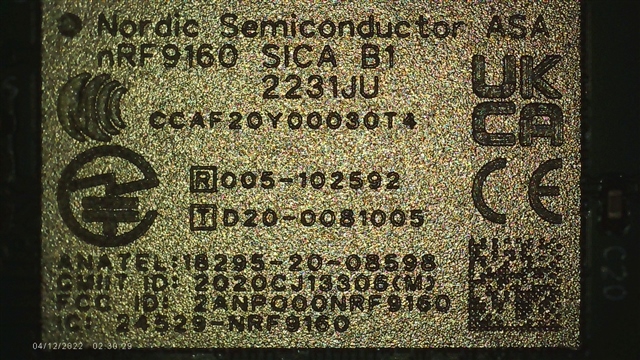
    I also attached a image of the NRF9160 devices from batch 1 

  • JLC has confirmed they bake PCB components at 60°C for 48 hours to remove moisture but can’t use higher temperatures. 

  • Hi,

    Håkon is not avaliable this week, I will help you on this ticket.

    I have checked the trace codes 2231JU and 2227FR, and both appear to be fine, with no similar issues reported previously.
    "JLC has confirmed they bake PCB components at 60°C for 48 hours to remove moisture but can’t use higher temperatures" -> is this in tray or in the reel? Please pay attention the reel can't withstand more than 40 C.

    Regarding the schematic and Gerber files, I am uncertain if Håkon has reviewed them. I will request a colleague to take another look to double-check.

    Additionally, I have a few suggestions for your hardware debugging:

    1. Ensure that the power system outputs the correct voltage as expected; if necessary, cut and resolder connections.
    2. Try to power on the nRF9160 standalone to observe its behavior.

    If the issue persists, we may request that you send in some of the problematic boards for further analysis.

    Best regards,

    Charlie

  • Hi Charlie, 

    Thanks for your reply. I modified the design a bit so it should be more easy to solder. In discussion with JLC I also choose for ENIG surface finish instead of HASL. 

    I expect the new boards beginning next week, I will update this post with the results. 

  • Hi Thijs,

    I see that the layout files are attached to the top of this ticket. Please also share the schematics for a review. You may upload PDF, Altium, Cadence and Gerber files by dragging a zipped folder to the text input field.

Related