Impedance Control nrf9151 RF Design

Hello,

It has been a while since I have done any controlled impedance and was wondering if someone could provide me a quick sanity check before I continue:

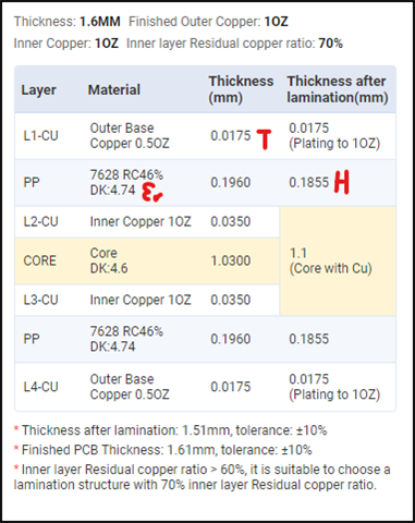
Here is the board stack up. I am using the top copper(L1) as waveguide and L2 as ground:

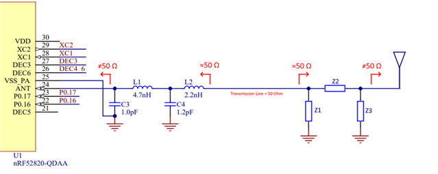
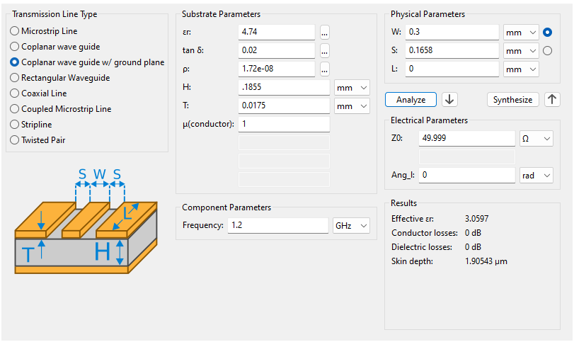
Here is the calculation. Chose 0.3mm trace width to keep manufacturing costs low.

It looks fine to me but after looking at the DK I am starting to question myself. First question is, the 50 Ohm trace is very thin and then transitions to a thicker trace. Do I need to be transitioning trace widths too?

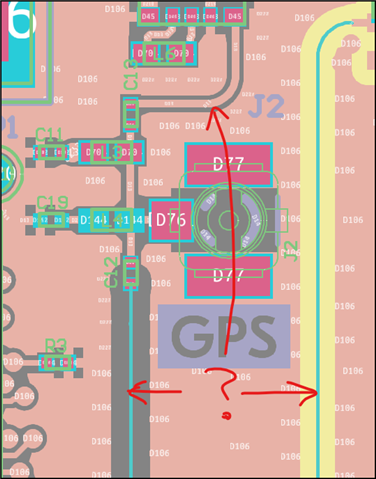
Second question, the GERBER file from the DK shows that there is ground immediately below on layer 2 meaning the "H" parameter should be relatively close to my calculation. How did the DK get the trace width W=0.1mm and Spacing S=0.41? To get those values using KiCad's calculator, you need a very thick board.

Parents
  • Sorry about the wait Doug, I guess this sanity check wasn't as quick as you've hoped.

    I had a talk with the designer behind the 9151DK. 

    L1-L2 distance should be ~0.075mm. Unless you are 100% replicating the pcb there is no need to do the transition. Our recommendation to all impedance related question is to specify what impedance you want and ask your manufacturer to adjust the final dimensions to fit the build. We also rely on our manufacturers to control impedances for us.

    It seems like you know what you are on the right path, though some input from your manufacturer would probably help. 

    Regards,

    Elfving

  • Thank you.

    I mostly wanted to use the reference design to confirm my calculations. I will have this conversation with my manufacturer and see what they recommend. 

    I have also looked at the NRF9160DK and that dev kit is making more sense on how traces are laid out. 

Reply Children
  • Doug K said:
    I have also looked at the NRF9160DK and that dev kit is making more sense on how traces are laid out. 

    Great, yeah it might be better to have a look at that. The 9151DK stands out a bit.

    According to the designer we change the trace width on that for a very silly reason related to particularities of the stack-up we have there (mainly L1-L2 distance is dictated by laser vias from L1 to L2). If you do not need laser vias then choose another configuration or materials. You shouldn't need to worry about this or width changes, just keep one that gives you 50Ω. 

    Let me know if there is anything else.

    Regards,

    Elfving

Related