NRF52832 Schematic Review

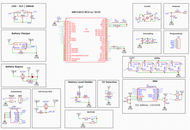
As the title suggests, I'd like some help reviewing my schematic for a 52832 pcb. I have tried to stay as close as possible to the DCDC reference design. 
Some notes on the uncommon parts:
- The STAT output on the battery charger is open drain or high Z
- The LED pin (LED data in) is not tied to the LED supply voltage
- All non-MCU supporting parts are moved over from a confirmed working design that was using an Espressif chip

Parents
  • A Quick observation reveals that the schematic is missing caps C13 & C14 at P0.26 & P0.25, respectively, according to the reference design.

    Moreover, check VCC LDO that it can still regulate after diode's forward voltage drop.

    Further, your adc VDRs comprise high impedances that may not be of much concern.

    Regards

    Shahid

Reply
  • A Quick observation reveals that the schematic is missing caps C13 & C14 at P0.26 & P0.25, respectively, according to the reference design.

    Moreover, check VCC LDO that it can still regulate after diode's forward voltage drop.

    Further, your adc VDRs comprise high impedances that may not be of much concern.

    Regards

    Shahid

Children
Related