Review PCB design for nrf54l15 for Matter over Thread use

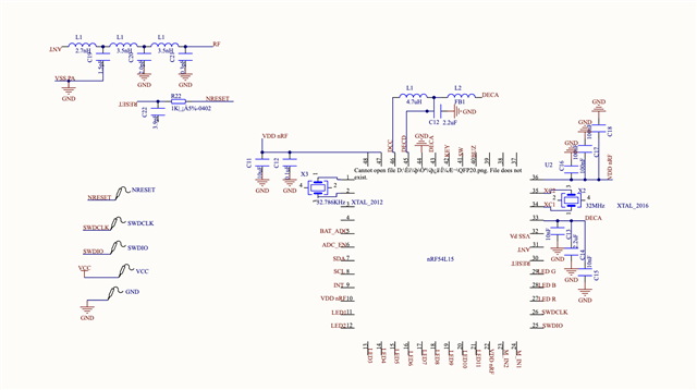
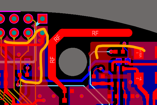
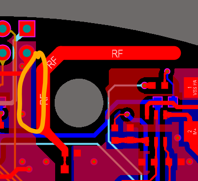
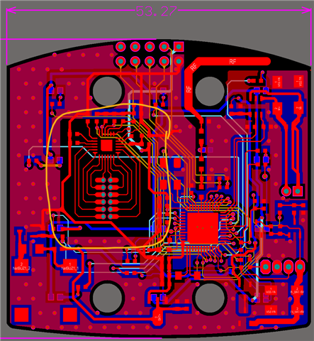
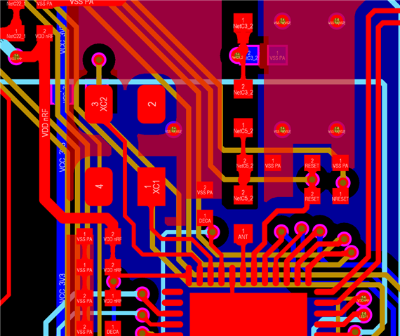
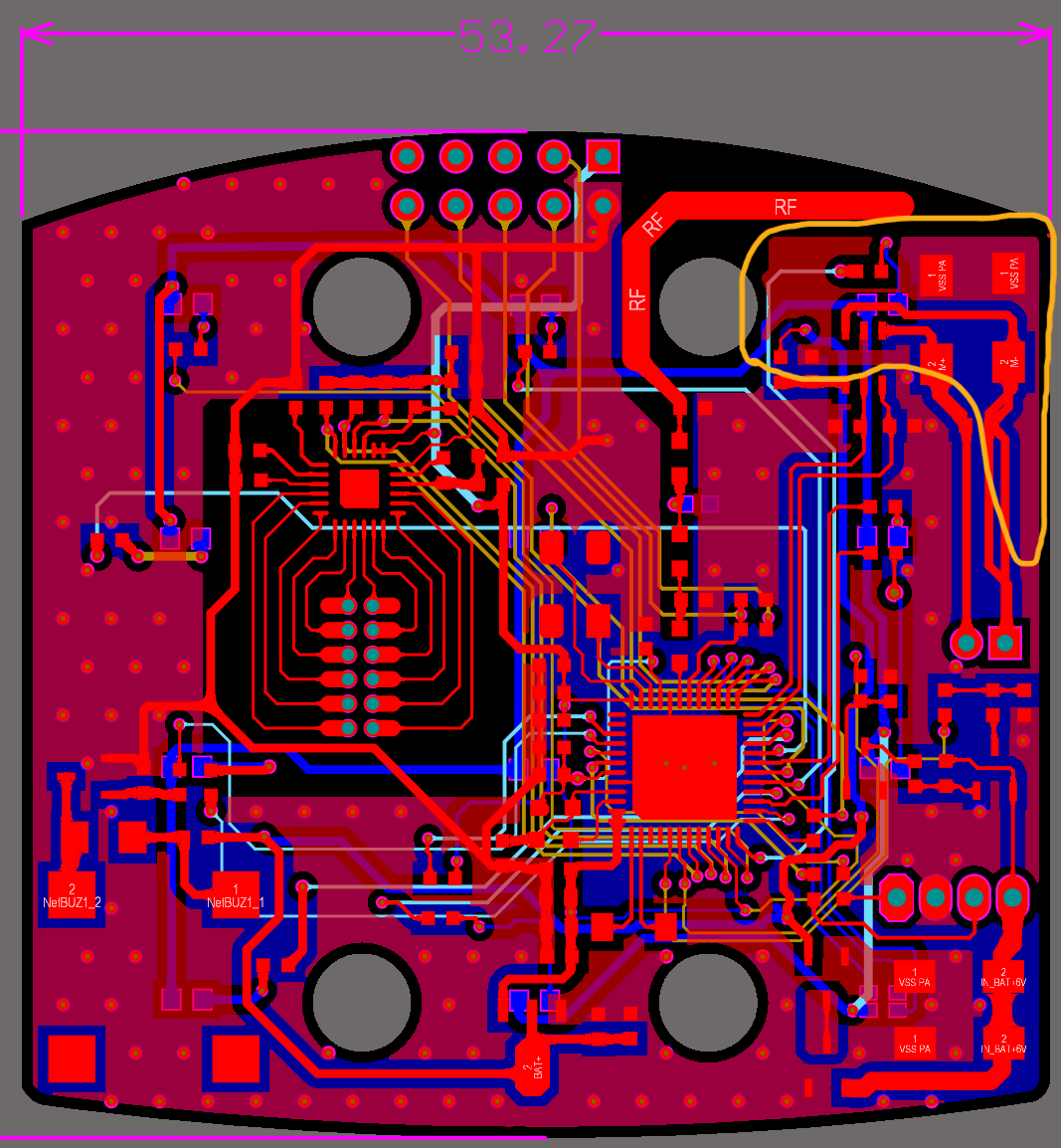
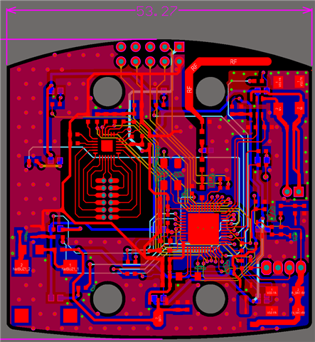
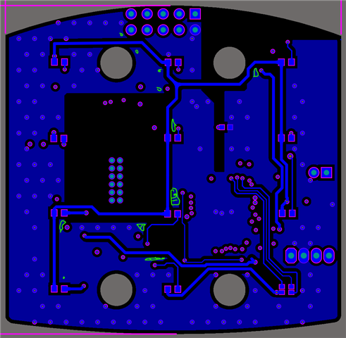
Hi, I would like to have some suggestions on my PCBA design for nrf54L15 chip. Please review it and give some suggestion moving forward. I am making this PCB to use this with matter-over-thread products. Since nrf54L15 is a pretty new product, I couldn't find many reference designs online. I mostly used the reference designs provided by Nordic but have been struggle on the programming port design. Also does nordic have any recommendation on which Antenna I should use for this design?

Thanks

  • Hi Eric, sorry for the delay, I will get back to you later today.

  • Eric Xin said:
    design.PcbDoc

    Schematic review

    • Antenna matching components are missing. For a trace antenna, it is common to use one shunt component. Place the component close to where the trace antenna leaves the ground plane. Some designers use a Pi-network, however, one components could be enough.

    Layout review

    • Use a cut-out below the RF-path, in the to first layers.
    • Add a ground plane all the way along the cut-out in the two inner layers.
    • Keep a ground plane underneath the RF-path. Make sure there ground plane is continous in the area below the RF-path.
    • Do not route any signals below the RF-path unless there is a ground plane in between.
    • Copy the reference design layout 1:1 when it comes to placement of the radio matching circuitry. Pack the components as close together and as close to the nRF as possible.
    • C19, the 1.5 pF capacitor should be grounded to VSS_PA only. In other words, C19 should be grounded only to the SoC ground pad. This provides additional filtering. See the reference layout.
    • Use a 50Ohm coplanar waveguide in between the radio matching circuitry and the antenna matching circuittry. You may use some sw to calculate the trace width and you may ask the pcb manufacturer for the dielectric constant of your particular FR-4. See the mentioned General PCB design guidelines for nRF52 series for a note on coplanar waveguides.
    • The trace antenna needs 5mm clearance next to it. The ground plance marked with orange are too close. See nWP008 and the mentioned guidelines.
    • What is the gray dot next to the antenna? Avoid screews close to the antnena.
    • No copper should be below or above the antenna. See the blue ground plane marked with orange:
    • Vias are missing from the ground pad. Copy the 16 vias from the reference design.
    • Why is there no ground below U2? Have you doubled checked with the documentation or component manufacturer that this is recommended? You could in any case try to ask the manufacturer for a review.
    • Avoid noisy signals below the 32MHz crystal or crossing the XC1 and XC2 traces. Use a ground plane between the crystal and any traces.  
    • Use vias to ground on the top layer ground planes here:
    • Make sure use a vias to ground on any ground plane stubs to avoid having them radiate like little antennas. See suggested vias in green below. Consider removing the ground plane areas suggested with dark green, or ground these areas with a via to ground.
    • Remember to stitch vias to ground close to the cut-out and close to the RF-path.
    • Make sure to connect stubs in bottom layer ground to top layer ground as well, using the suggested vias in green, or remove the areas suggested in green:
    • Keep decoupling capacitors as close to the SoC as possible. (I have not checked this). See the reference layout.
Related