
Hi there,
We have a device that utilizes an NRF52840 chip. Several threads on DevZone - including this one and this one - warn about the dangers of applying voltage to a GPIO while the device is unpowered. Doing so could back-power the device and create issues such as the inability to perform a power-on reset, or even permanent damage.
We have accidentally created this scenario, but have not seen any problems and I’m curious as to why. I may have figured it out, but not sure.
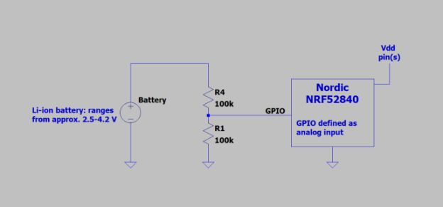
Here’s our situation: we are monitoring a battery voltage using a resistive voltage divider, as shown below in a simplified version of our schematic. (I’ve left out things like the on/off switch, the regulator that powers the NRF52840, etc.) The output of the voltage divider feeds a GPIO that is defined as an analog input. Because the battery is always connected to R4, the GPIO voltage is always present - regardless of whether or not the Nordic chip has power.
I took measurements to help understand the situation. I used a benchtop power supply in place of the battery and varied it from 0 to 4.2 V. I didn’t turn our device on so that the NRF52840 would be unpowered (i.e. Vdd = 0). I measured the voltage at the GPIO pin and the Vdd pin. I also used these voltages & the nominal resistor values to calculate currents. The results are shown below.
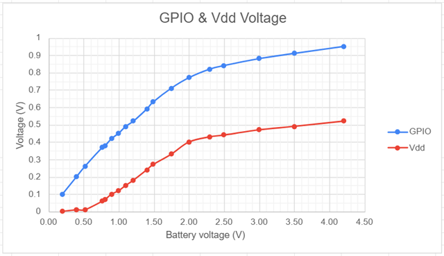
Chart 1
Chart 1 - things to note:
- The GPIO voltage isn't linear. Not too surprising. You’d expect a linear response if the circuit was acting like an ideal voltage divider - but we know it isn't.
- The Vdd pin never gets high enough to power up the Nordic chip. The minimum operating voltage for the NRF52840 is 1.7 V, and Vdd is only getting to ~0.5 V.
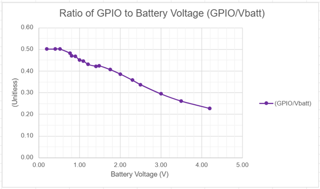
Chart 2
Chart 2 - things to note:
- This ratio isn’t flat. Again, not a surprise. If we had an ideal voltage divider with two equal resistors, we should see a flat line at 0.5 V because the output of the voltage divider would be half of the input. Clearly we don’t see that.
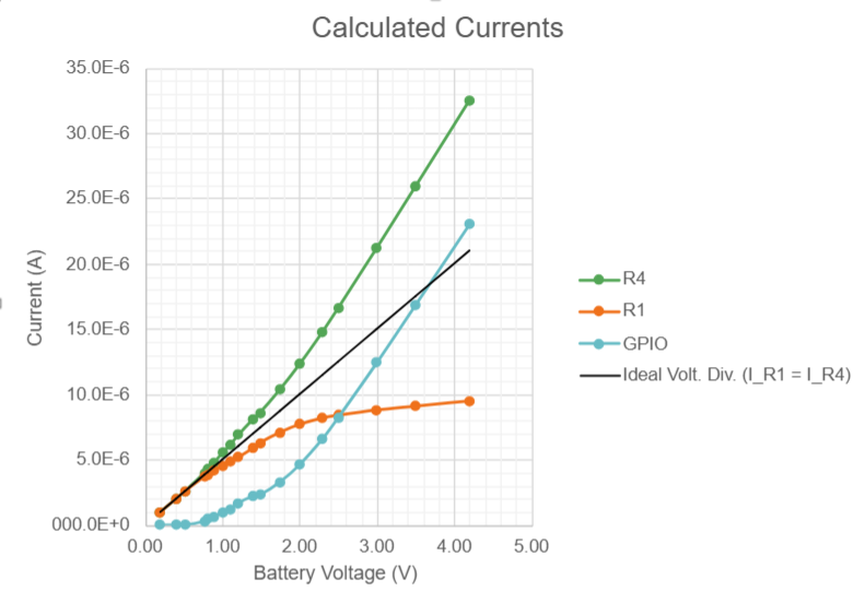
Chart 3
Chart 3 - things to note:
- For battery voltages up to 0.8 V, the circuit acts like an ideal voltage divider (GPIO current is zero; currents through R1& R4 are equal). At a battery voltage of 0.8 V, however, current begins to flow into the Nordic GPIO pin. (Note from the first chart that when the battery is at 0.8 V, the GPIO voltage is 0.4 V. Perhaps 0.4 V is enough to turn on an internal diode?)
- The total current flowing into the GPIO pin is very small (uA) - likely because of the 100k resistor R4. This probably prevents any permanent damage from occurring.
- Because the GPIO pin is drawing current, more leakage than necessary will occur when the Nordic chip is powered down. This will drain the battery faster during extended periods of off time.
So, that’s my story. 
I’d appreciate any insight regarding why we haven't been seeing problems. Maybe I've figured it out, maybe I haven't. I’d especially like to know more about what’s happening internal to the GPIO pin - like what is actually turning on & conducting. Is it an ESD protection diode, as some threads state?
Thanks!
Steve
