nrf52840 HFXO PCB Stray Capacitance

Hello,

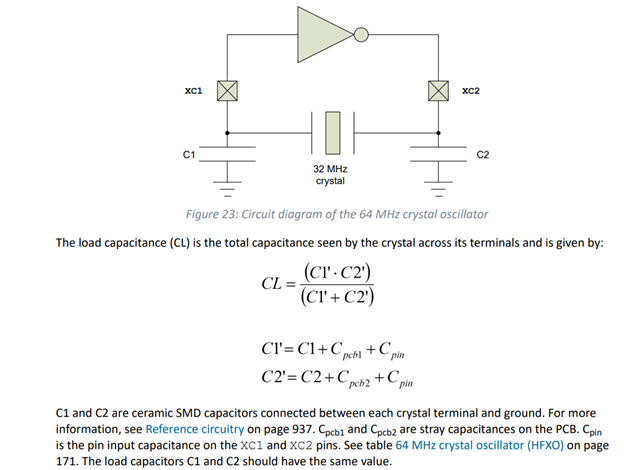
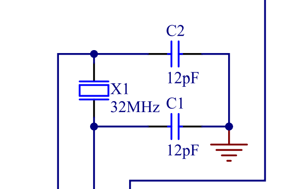
I am currently designing with the nrf52840 and trying to implement the 32 MHz crystal required for bluetooth radio operation. The calculations for the load capacitance given on your datasheet on page 159 have left me a bit confused. What is meant by the PCB stray capacitance and how can we calculate this? No help is given at all in the datasheet for what this means or how to calculate it.

Parents
  • Hi,

    The PCB stray capacitance are the capacitance of the traces connecting XC1 and XC2 to the crystal. If the traces are kept short the capacitance can be assumed to be 0pF, as it will not have a significant impact on the total crystal load capacitance.

    If you assume C_pcb1 = C_pcb2 = 0pF and C1 = C2 = C, the equation in the datasheet can be simplified to:

    C = 2 * CL - C_pin

    This gives a good starting point, which can be fine tuned by measuring the frequency offset of the radio. The radio frequency accuracy is directly dependent on the accuracy of the crystal oscillator, where the oscillating frequency of the crystal is dependent on the load capacitance.


    Best regards,

    Bendik

Reply
  • Hi,

    The PCB stray capacitance are the capacitance of the traces connecting XC1 and XC2 to the crystal. If the traces are kept short the capacitance can be assumed to be 0pF, as it will not have a significant impact on the total crystal load capacitance.

    If you assume C_pcb1 = C_pcb2 = 0pF and C1 = C2 = C, the equation in the datasheet can be simplified to:

    C = 2 * CL - C_pin

    This gives a good starting point, which can be fine tuned by measuring the frequency offset of the radio. The radio frequency accuracy is directly dependent on the accuracy of the crystal oscillator, where the oscillating frequency of the crystal is dependent on the load capacitance.


    Best regards,

    Bendik

Children
Related