VBUS_nRF Switch on nRF7002 DK

Hello,

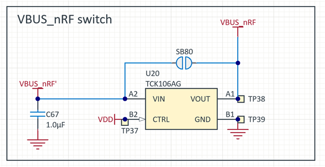
I am developing custom hardware based on this DK and am trying to eliminate circuitry that is unnecessary to my application. The DK includes a U20 load switch which automatically turns on when USB VBUS is applied. The DK also provides a solder bridge bypass option. I am unable to find a sequencing specification in the nRF5340 datasheet that says VDD must be applied before VBUS. The presence of this switch implies there is a sequencing requirement. So, I guess my question is, is this switch necessary for a minimal application hardware scenario? If I remove this switch then VBUS could come up before VDD. Would this present a reliability problem? How about if VBUS were present with VDD no applied at all?

Thank you,

Chris

Parents
  • Hi Chris

    The sequencing of power is only important for the nRF7002. From the nRF7002 product spec:

    "14.3.5 Supply sequencing requirements

    The various supplies and BUCKEN need to be sequenced in order with delay requirements. The power up sequence and requirements are:

    •  Supply VBAT/BUCKVBAT/BUCKVBATS/AFEVBAT
    • Wait ≥ 6 ms
    • Assert BUCKEN
    • Wait ≥ 1 ms
    • Supply IOVDD"

    If VBUS reaches a valid range and VDD isn't supplied, the system will not start up.

    Best regards,

    Simon

Reply
  • Hi Chris

    The sequencing of power is only important for the nRF7002. From the nRF7002 product spec:

    "14.3.5 Supply sequencing requirements

    The various supplies and BUCKEN need to be sequenced in order with delay requirements. The power up sequence and requirements are:

    •  Supply VBAT/BUCKVBAT/BUCKVBATS/AFEVBAT
    • Wait ≥ 6 ms
    • Assert BUCKEN
    • Wait ≥ 1 ms
    • Supply IOVDD"

    If VBUS reaches a valid range and VDD isn't supplied, the system will not start up.

    Best regards,

    Simon

Children
Related