Hi!
I have just received the nRF52840DK board and am currently perusing its schematics. Please don't be annoyed by my following question, but there are things I'm quite bewildered about.
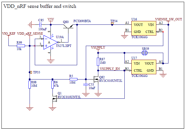
The schematics uses load switches TCK106AG. But sometimes they connected in a weird way. For example, U16 - this one is used in the part of VDD_nRF sense buffer. This buffer is definitely having the TP34 as output from emitter of bipolar transistor Q80, which is controlled by voltage from operational amplifier U19A - to create same voltage as the reference level VDD_nRF_SENSE. In this way Nordic implements 'repeater', so the generated voltage is of the same level as VDD_nRF_SENSE, while the actual power is drawn from the 5V rail. Here everything is clear, but then TP34 goes to OUT of TCK106AG (U16) and IN of TCK106AG (U16) goes to VSENSE_SW_OUT. By all logic at TP34 we have the generated voltage which must go to VSENSE_SW_OUT. But instead we have OUT and IN reversed.
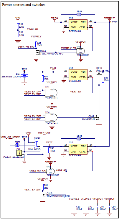
Same weird reversed connection is implemented on U13, U14, U15 where clearly by logic we see VREG, VBAT and VEXT are to be routed to output, to be merged at VSUPPLY. So logically, I'd expect VREG, VBAT, VEXT to be connected to IN pins on their respective TCK106AG-s, while OUTs to be merged into VSUPPLY.
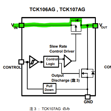
Is it some trick using TCK106AG, or TCK106AG is just a bidirectional device, so IN OUT are interchangeable? Though by TCK106AG's PDF, the IC uses a single P-Channel MOSFET which connects IN to OUT. As far as my knowledge lets me, a turned on MOSFET conducts from drain (D) to source (S).
So I'm totally lost here. Please somebody explain what happens?